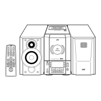
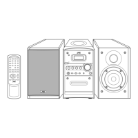
Do you have a question about the JVC UX-V10GN and is the answer not in the manual?
Performs isolation check on exposed metal parts for electrical shock hazards.
Uses an AC voltmeter and resistor/capacitor to measure leakage current.
Details on laser product warnings and label reproduction.
Instructions for removing the rear cover and side panels of the main unit.
Procedure to detach the cassette mechanism assembly.
Steps to remove the main board and its associated heat sink.
Procedures for removing the front panel and headphone board components.
Steps for removing the tuner board, power transformer, and AC supply board.
Procedure to remove the Opt.Dig.out board from the cassette mechanism.
Steps to remove the main cassette mechanism assembly.
Instructions for removing the CD mechanism assembly and its cover.
Procedure to remove the LED board (A).
Steps for removing LED board (B), door switch, servo control, motor, LCD, and operation boards.
Procedure for removing the playback/recording and eraser head assembly.
Steps for correctly reassembling the playback/recording and eraser head.
Procedure to remove the head amplifier and mechanism control PC board.
Instructions for removing the main motor assembly and related parts.
Procedure for removing the flywheel components.
Steps to remove the reel pulse PC board and solenoid.
List of instruments needed for performing adjustments and measurements.
Specifies measurement conditions and radio input signal parameters.
Details for adjusting the tuner section across different versions.
Important considerations and warnings during measurement procedures.
Diagrams showing adjustment points on the cassette mechanism.
Diagrams indicating adjustment points on the front panel assembly.
Procedure to confirm head angle using test tape VTT703L.
Procedure to confirm tape speed using test tape VT712.
Reference values for tape speed difference and wow & flutter.
Procedure to adjust recording bias current for Lch and Rch.
Adjustment for output deviation between 1kHz and 10kHz.
Reference values for recording bias frequency and eraser current.
Instructions for cleaning the laser pickup lens with an alcohol swab.
Symptoms indicating a worn-out laser diode and RF output checks.
Information regarding the semi-fixed resistor for laser power adjustment.
Diagrams showing the pin layout and internal block structure of the LA6541 IC.
Detailed description of each pin's function for the LA6541 IC.
Overview of the terminal layout for the MN35510 IC.
Internal block diagram illustrating the MN35510 IC's functionality.
Detailed description of each pin's function for the MN35510 IC.
Pin layout diagram for the AN8806SB-W IC.
Block diagram illustrating the AN8806SB-W IC's circuitry.
Detailed description of pin functions for the AN8806SB-W IC.
Comprehensive list of pin functions for various integrated circuits.
Pin layout diagram for the UPD78064GF-108 System CPU IC.
Detailed pin function descriptions for the UPD78064GF-108 IC.
Block diagram for the LA1838 FM/AM IF AMP & Detector IC.
Detailed pin function descriptions for the LA1838 IC.
Pin layout diagram for the LC72136N PLL Frequency Synthesizer IC.
Block diagram for the LC72136N PLL Frequency Synthesizer IC.
Detailed pin function descriptions for the LC72136N IC.
Pin layout for the BA15218N Dual Op. Amp.
Block diagram for the BA15218N Dual Op. Amp.
Pin layout for the BU4094BCF-X Serial to Parallel Port Extension IC.
Block diagram for the BU4094BCF-X Serial to Parallel Port Extension IC.
Pin layout for the GP1U271X Receiver for Remote IC.
Description of pin functions for the GP1U271X Receiver for Remote IC.
Pin layout for the LB1641 DC Motor Driver IC.
Description of pin functions for the LB1641 DC Motor Driver IC.
Block diagram for the AN7345 PB/REC AMP IC.
Detailed pin function descriptions for the AN7345 IC.
Pin assignment diagram for the LC75342 IC.
Block diagram for the LC75342 IC.
Detailed list of pin functions for the LC75342 IC.
Pin assignment diagram for the LC72723 IC.
Block diagram for the LC72723 IC.
Detailed description of pin functions for the LC72723 IC.
| CD Player | Yes |
|---|---|
| Tuner | Yes |
| Preset stations quantity | 30 |
| Bluetooth | Yes |
| USB Port | Yes |
| Number of channels | 2 |
| Tuner type | Digital |
| Cassette deck | No |
| Supported radio bands | FM |
| Speaker type | 2-way |
| Playable media formats | CD, MP3 |