EasyManua.ls Logo

JVC XP-A1000BK - Page 22

JVC XP-A1000BK
73 pages
Print Icon
To Next Page IconTo Next Page
To Previous Page IconTo Previous Page
Loading...
XP-A1000BK
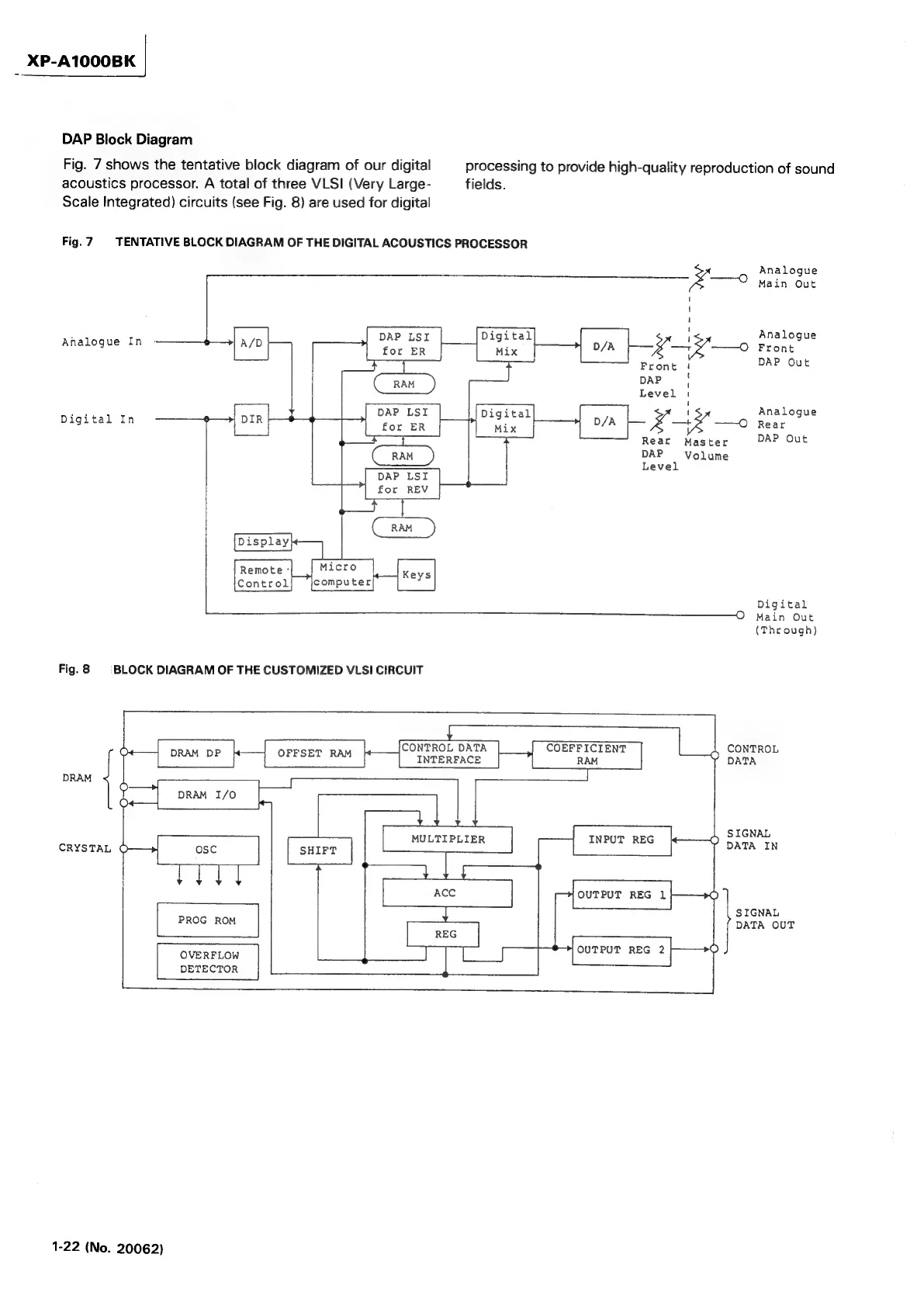
DAP
Block
Diagram
Fig.
7
shows
the
tentative
block
diagram
of
our
digital
acoustics
processor.
A
total
of
three
VLSI
(Very
Large-
fields.
Scale
Integrated)
circuits
(see
Fig.
8)
are
used
for
digital
Fig.7
TENTATIVE
BLOCK
DIAGRAM
OF
THE
DIGITAL
ACOUSTICS
PROCESSOR
Analogue
In
Digital
In
DAP
LSI
for
ER
DAP
LSI
for
ER
Fig.8
|
BLOCK
DIAGRAM
OF
THE
CUSTOMIZED
VLSI
CIRCUIT
CRYSTAL
O——»
osc
o—|
DRAM
DP
DRAM
a
eee
i
DRAM
I/O
a
aa
eae
PROG
ROM
OVERFLOW
DETECTOR
SHIFT
1-22
(No.
20062)
MULTIPLIER
processing
to
provide
high-quality
reproduction
of
sound
Analogue
O
Main
Out
i
Analogue
¥—¥—0
Front
DAP
Out
j
Analogue
cord
——O
Rear
Rear
Master
DAP Out
DAP
=
Volume
Level
Digital
Main
Out
(The
ough)
CONTROL
DATA
COEFFICIENT
CONTROL
pay
SIGNAL
INPUT
REG
©
DATA
IN
OUTPUT
REG
1
O
SIGNAL
DATA
OUT
OUTPUT
REG
2
9