EasyManua.ls Logo

JVC XP-A1000BK - Page 33

JVC XP-A1000BK
73 pages
Print Icon
To Next Page IconTo Next Page
To Previous Page IconTo Previous Page
Loading...
=
a
=
aS
b
o
cS
v
=a
voltage
source
7
Level
+
5
Comparator
conversion
circuit
r
Reference
Comparator
voltage
.
source
2
yl
Output
circuit
Address
input
XP-A1000BK
Line
and
column
address
buffer
bine
decoder
Column
decoder
Sense
refresh
amplifier
and
1/0
control
circuit
Memory
cell
(262,144
bits)
Vee(5V)
Vss(OV)
DQ:
0@2
0Q3
0a4
Data
input/output
Data
output
buffer
Mi
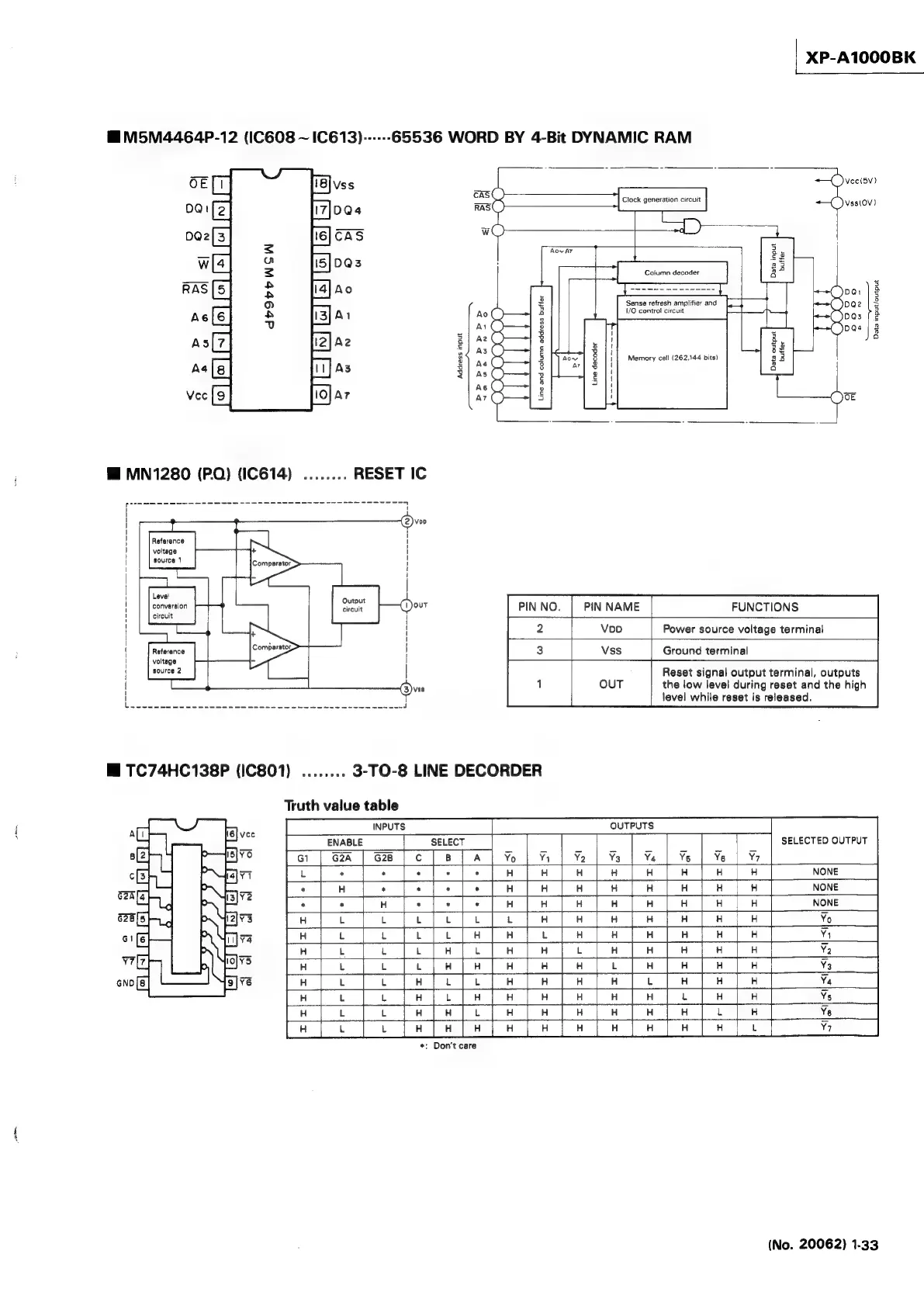
TC74HC138P
(IC801)
........
3-TO-8
LINE
DECORDER
Truth
value
table
<
a
o
INPUTS
OUTPUTS
ENABLE
SELECT
<
ol
G2A
4__-
Z|
N
oO
X\
°
xl
wl
a!
<I
S
at al
PIN
NO.
PIN
NAME
FUNCTIONS
Power
source
voltage
terminal
Ps
|
ves
|
Ground
terminal
Reset
signal
output
terminal,
outputs
the
low
level
during
reset
and
the
high
level
while
reset
is
released.
J
xl
~
SELECTED
OUTPUT
«|
*
~
NI
NONE
NONE
al
:
NONE
<
ul
ryxryrit
Yo
+
+
Y4
|
aI
|
<
a
al
X)/Xrler|xryrlycryTr
XTjyrjyxcl/
Tl]
ryT\=T
cabebaE
or
Ya
¥3
Lyric]
TyTrycrsyryT
|
Ya
XLie|e|x}yxr{[e|[eje
ay
|
Ys
Ye
Ce
Oe Oe Oe Oe
0
oe
ee
ecle[ole[rl[erjer
|
ol
cle
*;
Don’t
care
=x
|
xri{ryxryz
UpULyULyLy
LT]
Lie
|
cyrlT
xryxryxrly=z
xyxrjxrl=x
|
xr{yUrjeo;cryTl/Ti{T\=z
Si
Bo
Oe
ele
OO
a
Oe
Oe
Od Oe wd
Oe
pao
ed
Oe
-{/xryt
+
¥7
(No.
20062)
1.33