Port
Name
Pin
Name
I/O
FunctionPin
No
.
023 114 174 315 445 631
025 115 205 331 464 632
026 116 223 343 465 654
031 125 226 346 466 662
032 131 243 351 503 664
043 132 244 364 506 703
047 134 245 365 516 712
051 143 251 371 532 723
054 152 261 411 546 731
065 155 263 412 565 732
071 156 265 413 606 734
072 162 271 423 612 743
073 165 306 431 624 754
074 172 311 432 627
5
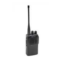
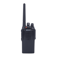
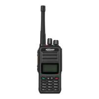
PT4200 SERVICE MANUAL
DCS
DCS (digital code squelch) is a kind of continuous digital code
modulated with voice signals on carrier wave to control squelch.
83 groups of standard codes (positive and inverse code) are
available. See table 3.2.
DCS signals generated by MCU (PWM wave shape) pass the
low pass filter to be filtered off the high frequency over 300Hz and
then are sent to VCO and TCXO for modulation. VCO modulates
the high frequency of DCS signals; TCXO modulates the low
frequency of DCS signals.
CTCSS/DCS signals from the receiver are sent to MCU for
modulation. MCU determines whether the DCS encoding of the
receiving signals is identical with that set on the radio and decides
whether to turn on the speaker.
Table 3.2 DCS Encoding List
3.7 Semiconductor Component
MCU Description
Table 3.3 Microprocessor (M38034) Port Description
1 TI P1 I
QT/DQT signal input
2 BUSY P2 I Busy s ignal in put
3 BATT P3 I Ba ttery vo ltage check
4 ALARM P4 I Alarm key check
5 TO P5 O QT/DQT output
6 BEEP P6 O Beep output/warning tone output
7
PF1
P7 I Voice indication key check
8
ENC0
P8 I Encoding input
9
ENC2
P9 I Encoding input
10
ENC3
P10 I Encoding input
11
ENC1
P11 I Encoding input
12
NC
P12 I Not used
13
PTT
P13 I [PTT] key input, connected with RXD
14
TXD
P14 O RS-232C input
15
RXD
P15 I RS-232C input
16
MONI
P16 I [MONI] key input
17 SELF P17 I Self programming
L: Model setting mode
18 CNVSS P18 I Connect 10K resistor with VSS
19 RST P19 I R e set i nput
20 INT0 P20 I P o w er ch eck in put
21 ENC P21 I
Encoding switch selection.
-SEL
Connect the pull down resistor with
VSS .
22 XIN P22 I 7.3MHz Osc illator
23 XOUT P23 O
24 VSS P24 I
Earthing
Clock frequency shift H Open
25 SHIFT P25 O
Final power supply H Open
26 PABC P26 O
VCO crystal selection.
27 OSCSI P27 I
Connect the pull down resistor with
VSS H 13 L 16.8
28 WNTC P28 O Wide/Narrow band contro l
H Wide L Narrow
29 PS P29 O PLL p ower s aving co ntrol H No rmal
working L Power saving
30 SDA P30 I/O EE PROM data wire
31 SCL P31 O EE PROM cloc k wire
32 UL P32 I PLL unlock che c k pin H Locked
L Loss of lock
33 DT P33 O PL L data output
34 CK P34 O PL L clock output
35 LE P35 O PLL IC en abl i n g pin H L atched
36 5MC P36 O Power control excep t CPU and
EEPROM L Open
37 AFCO P37 O
Audio amplification power H:Open
38 RX P38 O TX/RX VCO Se l e c tion H Rece iving
39 GLED P39 O Gree n indicato r contro l H Ligh t
40 RLED P40 O Re d indicato r contro l H Light
41 SAVE P41 O Battery power saving c o ntrol
H Power supply L Power saving
42 MUTE P42 O Squelc h contro l
H L Audio squelch
Mic squelch
43 5RC P43 O
eceiving power control L Open
R
44 5TC P44 O
Transmitter power control H Open
45 W588C P45 O
Voice indication H Voice
annunciation of channel
Alert control H Control by voice
46 AC P46 O
volume.
It must be in low battery
level
when in emergency alert state
.
D/A output 1
47 DAOUT1 P47 O
D/A output 0
48 DAOUT0 P48 O
D/A output 7 frequency regulated
49 DAOUT7 P49 O
output VCCN
50 DAOUT6 P50 O D/A output6
51 DAOUT5 P51 O D/A output5
52 DAOUT4 P52 O D/A output4
53 DAOUT3 P53 O D/A output3
54 DAOUT2 P54 O D/A output2
55 NC P55 O Not used
56 APC P 5 6
O
TX Auto
power
contro l outpu t
RX BPF tuning output
57 VCC P57 I CPU pow er 5V input
58 VREF P58 I Connected with VCC
P59
59 AVSS I Conn ecte d with VSS
60 IF_SEL
I
IF selection. Connect the pull down
P60
resistor with VSS H 49.95 L 21.4