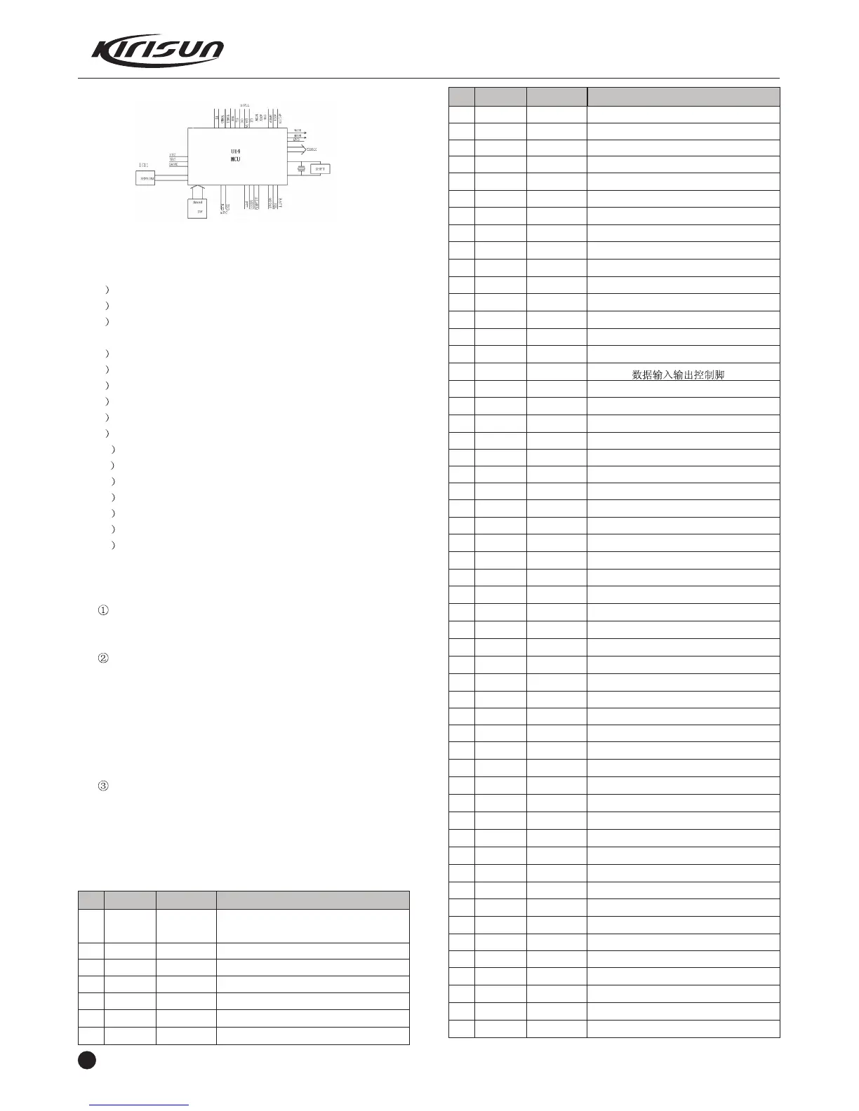
MCU controls the working of each unit of the radio to realize
all the radio functions.
1 Connects with the PC
2 Accesses the radio status data
3 Controls PLL to generate the receiving and transmitting local
oscillation frequency.
4 Accesses the current channel status.
5 Controls the LED status indication
6 Controls the power supply of each location
7 Checks the action of each function key
8 Generates voice contents
9 Generates power on voice prompt
10 Generates CTCSS/DCS signals
11 Generates 2 tone/5 tone signals
12 Generates power control signals
13 Completes CTCSS/DCS decoding
14 Completes 2 tone/5 tone decoding
15 Squelch check and control
16 VOX level sampling
Controls the audio processing chips to complete
emphasis/deemphasis, scrambling/descrambling, companding,
filtration and amplification etc.
2
Memorizer (E PROM, AT24C64)
Memorizes the channel data, CTCSS/DCS data as well as
other function setting data and parameter setting data of the radio.
CTCSS/DCS Encoding and Decoding:
CTCSS/DCS signals generated by MCU (pin24, pin28 output,
PWM wave) are filtered at the filter circuit and then sent to VCO and
TCXO modulation respectively.
CTCSS/DCS signals from the receiver are sent to MCU for
decoding. MCU determines whether the signals contain the same
CTCSS/DCS as that set on the radio and decides whether to turn
on the speaker.
Power adjustment:
MCU PIN1 output DC signals, inputted to APC unit to control
the output power of the transmitter.
3.8 Semiconductor Component
MCU Description
Table 3.3 Microprocessor (M30620FCPFP) Port Description
PinNo. Port Name
1 PCTV
2 DTMF
3 HSDI
4 EPDT
5 EPCK
6 BYTE
7 CNVSS
Input/ output
D/A Output
D/A Output
I
I/O
O
I
I
Function
Receiver sensitivity adjusting voltage
output/power control (V)
DTMF/Tone output, beep output
Tone decoding input
EEPROM data input/ output
EEPROM clock
Gnd
Gnd
8 BSHIFT
9SV
10 RESET
11 XOUT
12 VSS
13 XIN
14 VCC
15 NC
16 VDET
17 RDT
18 TCLK
19 SCLK
20 QT/DQT
21 TDATA
22 StCtrl
23 DI/O
24 QTVCO
25 DIR
26 APC
27 NC
28 QTTCXO
29 TXD
30 RXD
31 NC
32 APC SW
33 TXD0
34 RXD0
35 DC SW
36 TX W/N
37 RX SW
38 TX SW
39 NC
40 PLL UL
41 PLL STD
42 PLL DATA
43 PLL CLK
44 NC
45 RX W/N
46 EN1
47 EN2
48 EN3
49 EN4
50 EN5
51 W/N R1
52 W/N R2
53 AFCON
54 RX MUTE
55 A BUSY
56 A DATA
57 A SCLK
58 A MUTE
59 NC
60 ACC
61 NC
O
O
I
O
-
I
-
I
I
I
I
O
I/O
O
O
I
O
O
O
-
O
O
I
-
O
O
I
O
O
O
O
-
I
O
O
O
-
O
I
I
I
I
I
O
O
O
O
I
O
O
O
-
-
-
Clock beat frequency control
Min. volume control
CPU reset input
CPU reset output
CPU clock input
Voltage down detection
AK2346 MSK signal input
AK2346 MSK data transmission clock
AK2346 data transmission clock
CTCSS/DCS output
AK2346 MSK data transmission outp ut
Side tone volume control pin
CTCSS/DCS output VCO (PWM)
AK2346 IO control
Power control (U)
TXD1 output
RXD1 input
Power control output switch
Extension
Extension
Power control switch
Transmission bandwidth switch
Receiver VCO switch
Transmitter VCO switch
Phase-locked loop loss of lock check pi n
Phase-locked loop enabling control
Gnd
+5V
+5V
AK2346
NC
QT/DQT TCXO (PWM)
NC
Gnd
Phase-locked loop data output
Phase-locked loop clock
NC
Receiving bandwidth switch
UV band selection
Encoding switch input pin
Encoding switch input pin
Encoding switch input pin
Encoding switch input pin
Receiving IF bandwidth switch
Receiving IF bandwidth switch
Audio power amplifier enablingcontrol
Receiving mute switch
Number reporting chip control
Number reporting chip data output
Number reporting chip clock
Number reporting chip control
NC
+5V
NC
PinNo. Port Name Input/ output Function
Figure 3.11 MCU Diagram
3.7 MCU:
Outputs
PT7200 SERVICE MANUAL
4
 Loading...