62 VSS
63 NC
64 SELF
65 OPT S1
66 OPT S2
67 PIO3
68 PIO2
69 PIO1
70 PINT
71 TK1
72 PTT
73 Sk2
74 SK1
SP SW
75
MIC SW
76
R LED
77
G LED
78
5T C
79
5R C
80
5C C
81
P03
82
P02
83
NC
84
NC
85
MAN DOWN
86
BATT
87
RSSI
88
BUSY
89
VOX
90
QT/DQT IN
91
DTMF IN
92
AVSS
93
NC
94
VREF
95
AVCC
96
NC
97
MIC MUTE
98
99
100
-
-
-
I
I
I/O
I/O
I/O
I
I
I
I
I
O
O
O
O
O
O
O
O
O
O
-
I
I
I
I
I
I
I
-
-
-
-
-
O
O
O
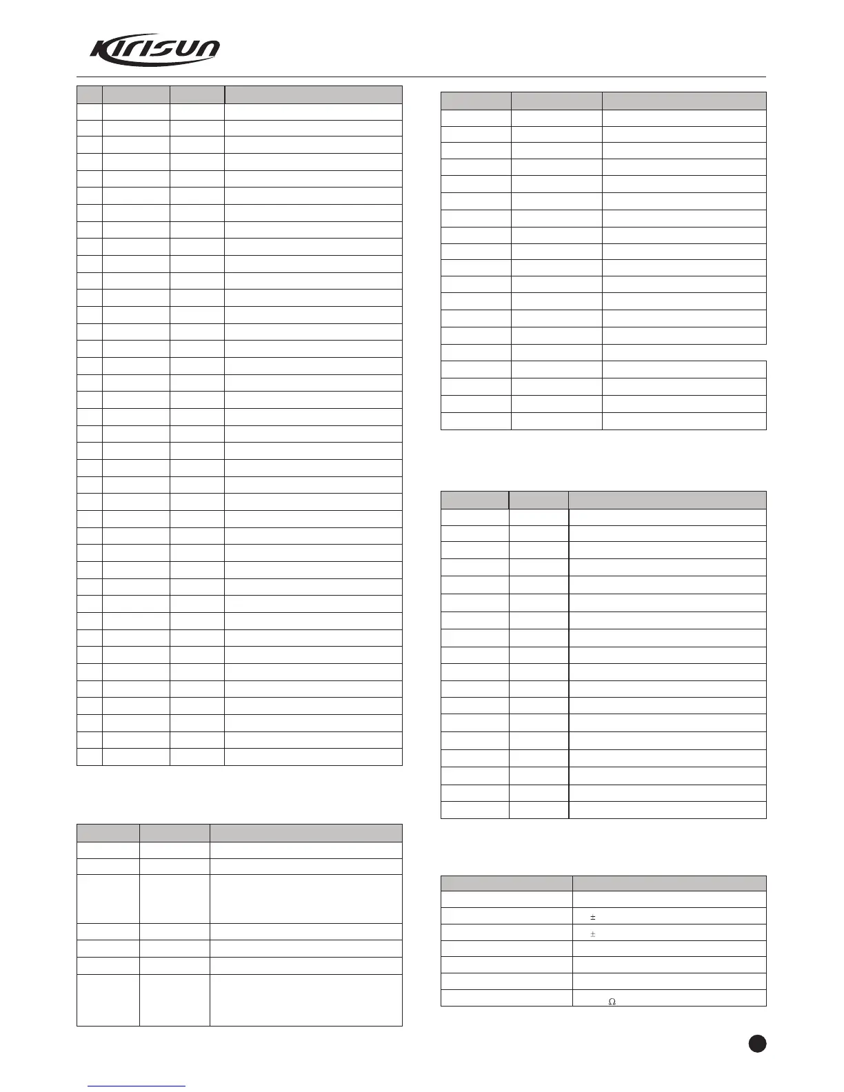
Table3.4: Semi-Conductor Component Function
U14 M30620FCPFP
U11 PST9140NR
Q60 2SC5108
Q66 2SC3356
Q56 2SC5108
Q57 2SC5108
Q65 2SC4617
Q77 2SC2412K
Q68 RD07MVS1
Q67 RD01MUS1
Q69 DTA144EE
Q79 3SK318
Q81 3SK318
Q78 2SC5108
Q73 DTC144EE
Q74 DTC144EE
Q83 2SJ243
Q76 2SA1745
Q85 2SJ243
Table 3.5 Diode Function Description
Location mark Model
D Ma77
D101 HSC277
D103 HSC277
D104 HSC277
D201 HSC277
D302 MA2S376
D304 MA2S376
D305 MA360
D310 MA2S376
D308 MA2S376
ZD12 HZU5ALL
D38 MA2S111
D48 MA2S111
D57 1N4148
D53 LED RED
D55 LED GREEN
D54 LED RED
D56 LED GREEN
Location mark Model Functiondescription
Table 3.6: XF203 crystal filter features
PinNo. Port Name Input/ output Function
MIC MUTE
HPF PC
Gnd
NC
Factory control options
Earphone check
External PTT
MAN DOWN input
Extension
Extension
Extension
Extension
Top key
PTT key
Side key 2
Side key 1
Speaker switch
MIC switch
LED red switch
LED green switch
5T control pin
5R control pin
5C control pin
Fixed side tone control
Phase-locked loop filter
NC
NC
Reverse detection input
Voltage check input
Receiving filed intensity signal input
Squelch voltage check input
VOX voltage check input
CTCSS/DCS input
DTMF input
Gnd
NC
+5V
+5V
NC
External and internal MIC switch
High pass filter switch
Function description
Phase-locked loop chip
APC, voltage comparison, drive
Receiver's 2nd local oscillation, 2nd IF
amplifier, amplitude limit, demodulation ,
noise amplification
Audio processing
MIC amplification
Receiver audio power amplifier
E2PROM, memory channel frequency
data, function setting parameter,
debugging status parameter
Location mark Model
Ic9 ADF4111
Ic10 NJM2904
U9 Ta31136
Ic12 AK2346
IC14 TC75W51FU
Q92 TDA8541
Ic11 AT24C64
MCU
MCU reset circuit
Transmitter 1st amplification
Transmitter 2nd amplification
VCO buffering amplifier
VCO buffering amplifier
VCO power filter
noise amplifier
Transmitter final amplifier
Transmitter amplifier drive
APC output switch
The first frequency mixer
Receiver HF amplifier
The first IF amplifier
Red LED drive
Green LED drive
C5V switch
T5V switch
R5V switch
Function Description
Transmitter antenna switch diode
VCO output switch
Antenna switch
Antenna switch
VCO output switch
VCO oscillation variable capacitance diode
VCO oscillation variable capacitance diode
VCO modulation diode
VCO oscillation variable capacitance diode
VCO oscillation variable capacitance diode
APC output voltage-limiting diode
Loss of lock check diode
VCO power filtering accelerating diode
Noise detector
Transmitting indication
Receiving indication
Transmitting indication
Receiving indication
Item
Nominal center frequency
Transmission bandwidth
40dB barrage bandwidth
Pulse
Insertion loss
Guarantee attenuation
Terminal resistance
Rated value
51.65MHz
7.5kHz or bigger within 3dB
20.0kHz or smaller
1.0dB or smaller
3.0dB or smaller
80dB or bigger within fo-910kHz
1.5k /6PF
PT7200 SERVICE MANUAL
5
 Loading...