Digital OverVoltage Relay (GDR-C01) User's Manual V1.00
Kyongbo Electronics Co., Ltd.
Order of Figures and Diagrams
【Figure 3.1】 OVR Logic Diagram ···································································································· 16
【Figure 4.1】 RS-232C Circuit Diagram ···························································································· 18
【Figure 4.2】 RS-232C Connection ····································································································· 18
【Figure 4.3】 RS-485C Connection Diagram ····················································································· 19
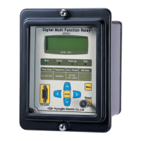
【Figure 5.1】 Front Panel Display ······································································································ 20
【Figure 6.1】 Menu Tree ····················································································································· 23
【Figure 7.1】 SetGDRSeries Default Screen ······················································································ 35
【Figure 7.2】 Relay Selecting ·············································································································· 37
【Figure 7.3】 Communication Port Setting ························································································ 37
【Figure 7.4】 GDR-C01 Setting ·········································································································· 39
【Figure 7.5】 GDR-C01 Status ············································································································ 40
【Figure 7.6】 GDR-C01 Report ··········································································································· 41
【Figure 7.7】 Help ································································································································ 42
Appended 1. Dimensioned Drawings - Unit : mm ············································································ 44
Appended 2. Internal Block Diagram ·································································································· 45
Appended 3. External Connection Diagram ························································································ 45
Appended 4. OverVoltage Element Inverse Time Characteristic Curve ·········································· 46
Appended 5. OverVoltage Element Definite Time Characteristic Curve ········································· 47