Installation
4-24
BA9300SU EN 2.1
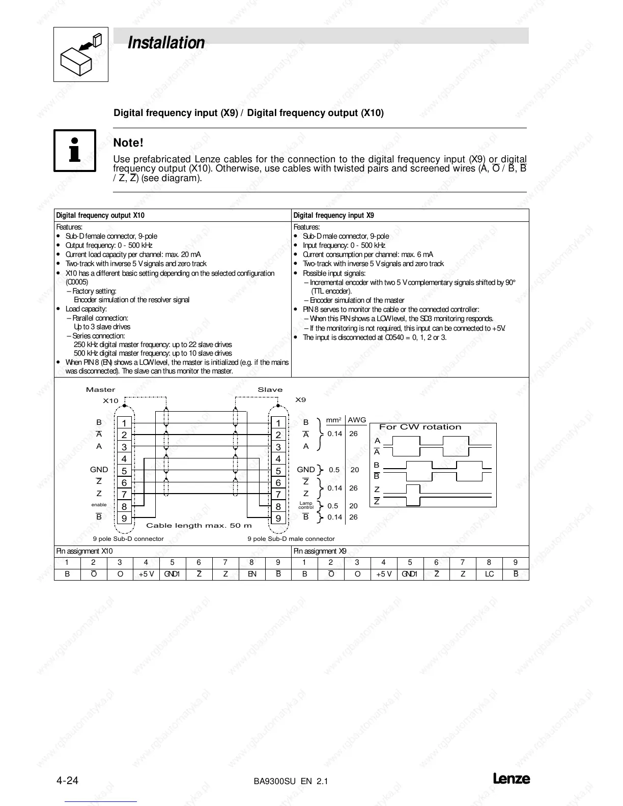
Digital frequency input (X9) / Digital frequency output (X10)
Note!
Use prefabricated Lenze cables for the connection to the digital frequency input (X9) or digital
frequency output (X10). Otherwise, use cables with twisted pairs and screened wires (A, O
/B,B
/Z,Z)(seediagram).
Digital frequency output X10 Digital frequency input X9
Features:
• Sub-D female connector, 9-pole
• Output frequency: 0 - 500 kHz
• Current load capacity per channel: max. 20 mA
• Two-track with inverse 5 Vsignals and zero track
• X10 has a different basic setting depending on the selected configuration
(C0005)
– Factory setting:
Encoder simulation of the resolver signal
• Load capacity:
– Parallel connection:
Up to 3 slave drives
– Series connection:
250 kHz digital master frequency: up to 22 slave drives
500 kHz digital master frequency: up to 10 slave drives
• When PIN 8 (EN)shows a LOW level, the master is initialized (e.g. if the mains
was disconnected). The slave can thus monitor the master.
Features:
• Sub-D male connector, 9-pole
• Input frequency: 0 - 500 kHz
• Current consumption per channel: max. 6 mA
• Two-track with inverse 5 Vsignals and zero track
• Possible input signals:
– Incremental encoder with two 5 V complementary signals shifted by 90°
(TTL encoder).
– Encoder simulation of the master
• PIN 8 serves to monitor the cable or the connected controller:
– When this PIN shows a LOW level, the SD3 monitoring responds.
– If the monitoring is not required, this input can be connected to + 5V.
• The input is disconnected at C0540 = 0, 1, 2 or 3.
1
2
3
4
5
6
7
8
9
1
2
3
4
5
6
7
8
9
B
A
A
GND
Z
Z
enable
B
B
A
A
GND
Z
Z
Lam p
control
B
Master
Slave
C able length m ax. 50 m
9 pole S ub-D connector
X10
X9
9 pole Sub-D m ale connector
A
B
F o r C W ro ta tio n
A
B
Z
Z
0.14 26
0.5 20
0.14 26
0.5 20
0.14 26
mm
2
AW G
Æ
Pin assignment X10 Pin assignment X9
1 2 3 4 5 6 7 8 9 1 2 3 4 5 6 7 8 9
B O O +5V GND1 Z Z EN B B O O +5V GND1 Z Z LC B