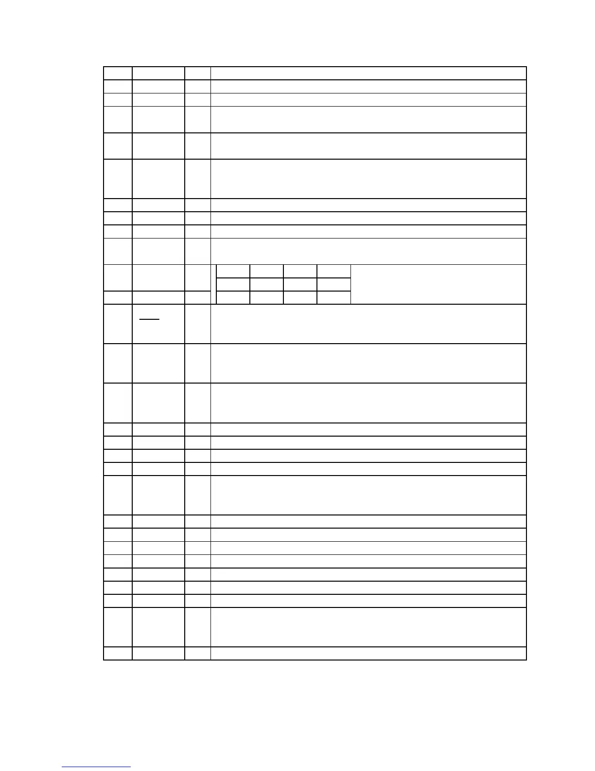
PIN SYNBOL I/O FUNCTION
1 DIN I Serial data input
2 BCKI I Bit clock input
3 XTIM I Select system clock frequency
Low = 256fs, High = 384fs
4 DITH I Dither select
Low = dither disable, High = dither added
Analog output stage gain
5 GAIN O Use only if Pin 19 is High
Low = low gain, High = high gain (+6dB)
6 XTI I System clock input
7 VDD1 - +5 volt power for filter
8 VSS1 - Ground
9 PROG I Select program mode
Low = Stand-alone, High = Program
16 Bits 18Bits 20Bits 24Bits
10 OSIZ0 I 0101
11 OSIZ1 I 0011
Output data format
12 COB I Low = complementary offset binary
High = 2's complement
Input data justification
13 JUST I Low = data assumed tobe left justified up to 24 bits in length
High = data right justified 16 bits
Input datalatching
14 BCPL I Low = input data latched on rising edge of BCKI
High = input data latched on falling edge of BCKI
15 SMUTE I Soft mute Low = off, High = on
16 DEEMPH I De-emphasis filter Low = off, High = on
17 HMUTE I Hard mute Low = off, High = on
18 FSEL I De-emphasis filter Fs Low = 44.1kHz, High = 48kHz
Gain scaling
19 SCAL I Low = 6dB gain scaling is performed internally in the digital domain
High = Analog output gain stage is set jby pin 5 GAIN
20 DG O DAC sample and hold deglitch signal
21 VSS2 - Ground (Common with VSS1)
22 VDD2 - +5V volt puwer for output interface
23 DOR O Right channel serial data output
24 DOL O Left channle serial data output
25 WCKO O Word clock output
26 BCKO O Bit clock output
HDCD encoding detect
27 HDCD O Low = no encoding, High = HDCD encoding input data
(Output current ratad at 12mA)
28 LRCI I Word clock input
Q510 : PMD-100
1-19