54
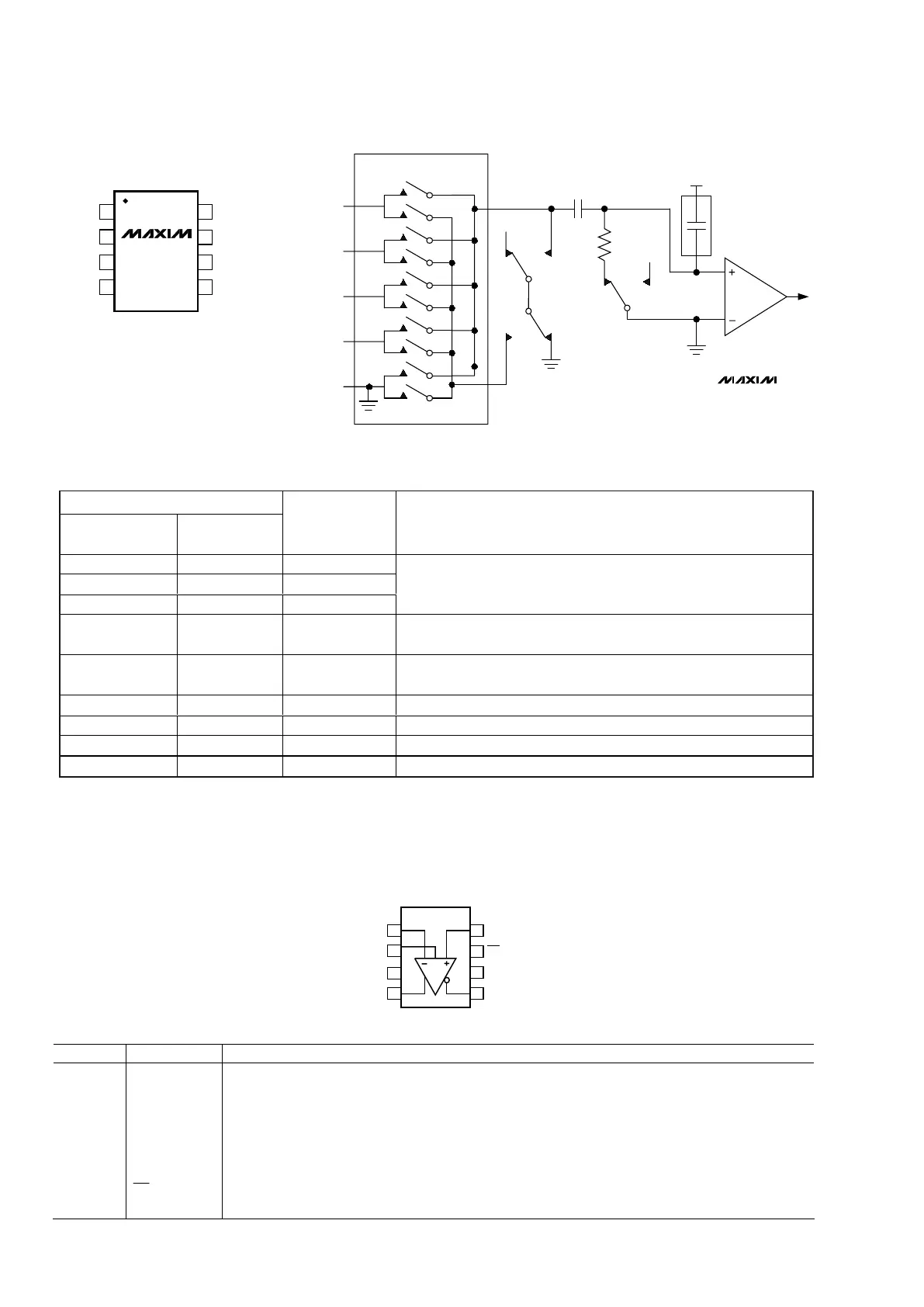
Q004 : MAX1037EKA+T (ADC)
TRACK
HOLD
C
T/H
TRACK
HOLD
DIFFERENTIAL
SINGLE ENDED
AIN0
AIN1
AIN2
AIN3/REF
GND
ANALOG INPUT MUX
CAPACITIVE
DAC
REF
MAX1036
MAX1037
Equivalent Input Circuit
SDA
SCLAIN3/REF
1
2
8
7
V
DD
GNDAIN1
AIN2
AIN0
SOT23
3
4
6
5
MAX1036
MAX1037
PIN CONFIGURATION
Top view
PIN
MAX1036/
MAX1037
MAX1038/
MAX1039
NAME FUNCTION
1, 2, 3 8, 7, 6 AIN0–AIN2
— 5, 4, 3, 2, 1 AIN3–AIN7
— 16, 15, 14 AIN8–AIN10
Analog Inputs
4 — AIN3/REF
Analog Input 3/Reference Input or Output. Selected in the setup
register.
— 13 AIN11/REF
Analog Input 11/Reference Input or Output. Selected in the setup
register.
5 9 SCL Clock Input
6 10 SDA Data Input/Output
7 11 GND Ground
812V
DD
Positive Supply. Bypass to GND with a 0.1μF capacitor.
PIN DESCRIPTIONS
Q654,Q655 : AD8137 (ADC ドライバ )
PIN CONFIGURATION
–IN
1
V
OCM
2
V
S+
3
+OUT
4
+IN
8
PD
7
V
S–
6
–OUT
5
AD8137
Pin No. Mnemonic Description
1 −IN Inverting Input.
2 V
OCM
An internal feedback loop drives the output common-mode voltage to be equal to the voltage applied to
the V
OCM
pin, provided the amplifier’s operation remains linear.
3 V
S+
Positive Power Supply Voltage.
4 +OUT Positive Side of the Differential Output.
5 −OUT Negative Side of the Differential Output.
6 V
S−
Negative Power Supply Voltage.
7
PD
Power Down.
8 +IN Noninverting Input.


 To Next Page