47
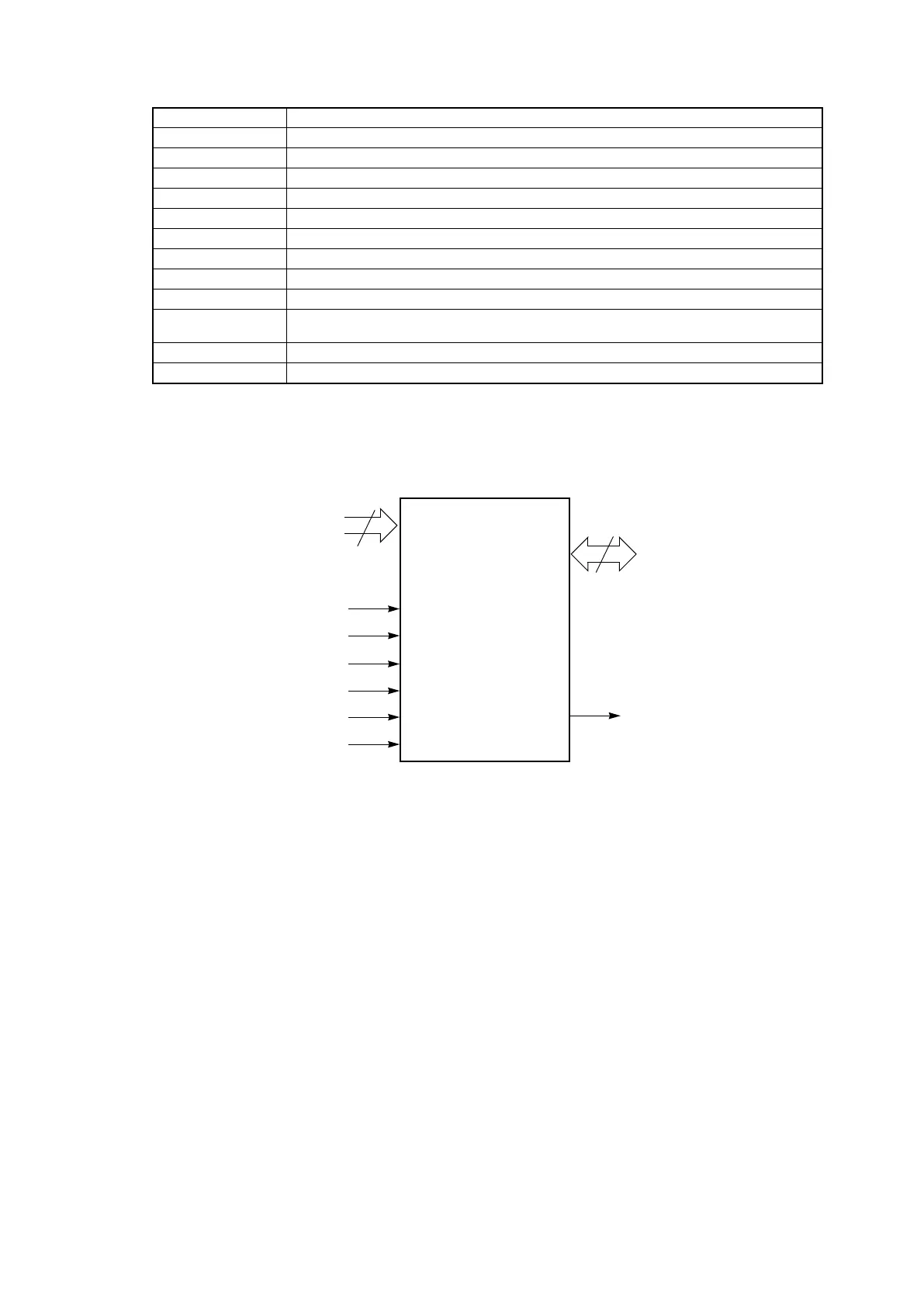
A0–A19 20 addresses
DQ0–DQ14 15 data inputs/outputs
DQ15/A-1 DQ15 (data input/output, word mode), A-1 (LSB address input, byte mode)
BYTE# Selects 8-bit or 16-bit mode
CE# Chip enable
OE# Output enable
WE# Write enable
WP# Write protect: The WP# contains an internal pull-up; when unconnected, WP is at V
IH
.
RESET# Hardware reset
RY/BY# Ready/Busy output
V
CC
3.0 volt-only single power supply (see Product Selector Guide on page 9 for speed options and voltage supply
tolerances)
V
SS
Device ground
NC Pin not connected internally
PIN CONFIGURATION
20
16 or 8
DQ0–DQ15
(A-1)
A0–A19
CE#
OE#
WE#
RESET#
BYTE# RY/BY#
WP#
LOGIC SYMBOL


 To Next Page