62
Q316 : XC9504B092AR (電源 IC)
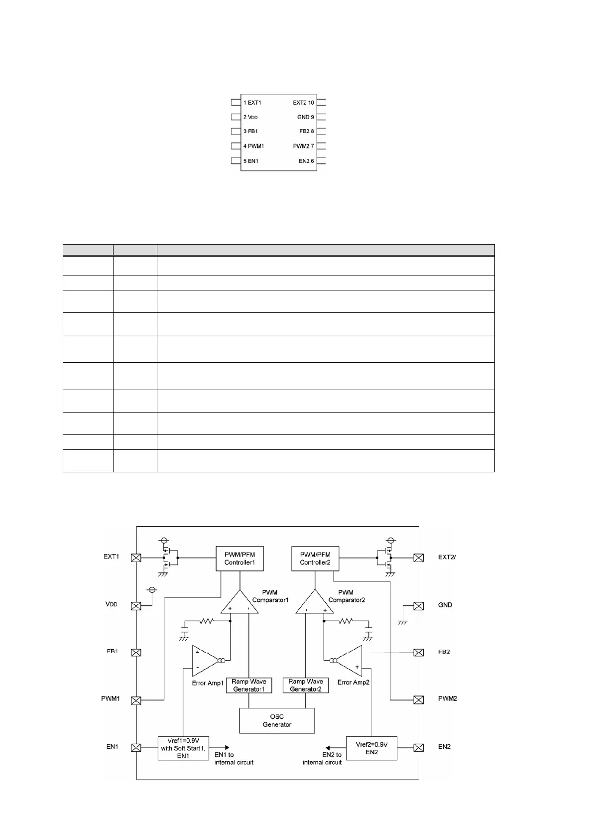
PIN CONFIGURATION
MSOP-10
(TOP VIEW)
PIN NUMBER PIN NAME FUNCTION
1 EXT 1
Channel 1: External Transistor Drive Pin
<Connected to N-ch Power MOSFET Gate>
2 V
DD
Supply Voltage
3 FB1
Channel 1: Output Voltage Monitor Feedback Pin <Threshold value: 0.9V. Output voltage
can be set freely by connecting split resistor between V
OUT1 and GND.>
4 PWM1
Channel 1: PWM/PFM Switching Pin <Control Output 1. PMW control when connected
to V
DD, PWM/PFM auto switching when connected to GND.>
5 EN1
Channel 1: Enable Pin <Connected to GND when Output 1 is in stand-by mode.
Connected to V
DD when Output 1 is active. EXT1 is low when in stand-by mode.>
6 EN2
Channel 2: Enable Pin <Connected to GND when Output 2 is in stand-by mode.
Connected to V
DD when Output 2 is active. EXT1 is high when in stand-by mode.>
7 PWM2
Channel 2: PWM/PFM Switching Pin <Control Output 2.PMW control when connected
to V
DD, PWM/PFM auto switching when connected to GND.>
8 FB2
Channel 2: Output Voltage Monitor Feedback Pin <Threshold value: 0.9V. Output voltage
can be set freely by connecting split resistor between V
OUT2 and GND.>
9 GND
Ground
10 EXT2/
Channel 2: External Transistor Drive Pin <Connected to P-ch Power MOSFET Gate>
PIN DESCRIPTIONS
BLOCK DIAGRAM
 Loading...