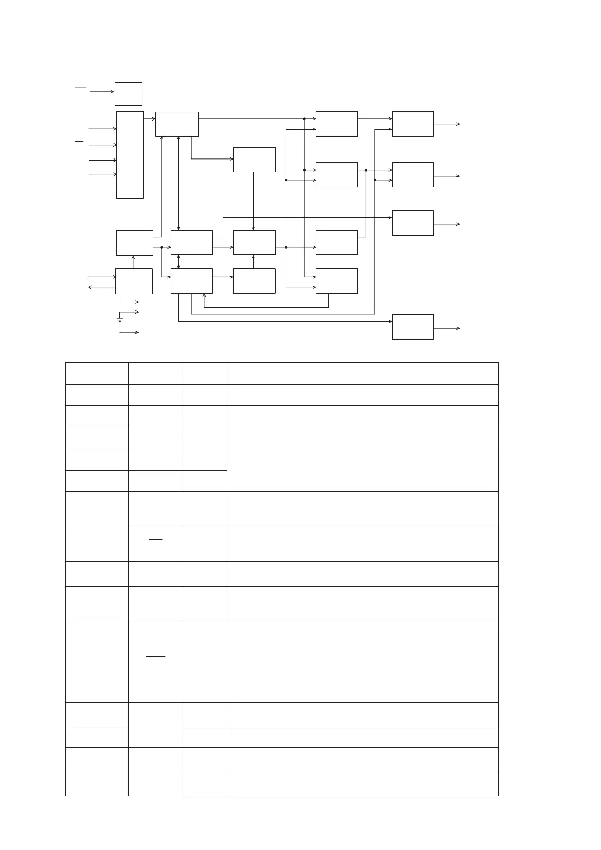
SI
CS
CL
K
R S
V
SS
OSC
1
OSC
2
V
D D
R S T
V
F DP
M K
1
~
M K
2
S
1
~
S
35
P
1
T
1
~T
1 6
8bits
Shift
Re g.
Instruction
D e
c oder
Timin
g
Gen.
C R
OSC .
State
Reg
.
Display
Control
Address
Selector
Read
Address
Counte
r
Line
Address
Counter
Timing
Driver
DD R A M
16x8 bit
CG R O M
8,400 bi
t
Port
Driver
CG R A
M
35x8 bit
Segment
Driver
M K R A
M
16x2 bit
Icon
Driver
RESET
No. SY M B O L I/O F U N C T I O N
57 V
D D
-
Po w er S ou rc e : V
D D
=+3.0 to 5.5V
49 V S S - G ND : V SS =0V
48 V
F D P
-
VFD Driv i n g Powe r S our s e
V
D D
-20V to V
D D
-45V
50 O S C 1 I
CR Oscillation Terminal
External R and C connect to these terminals.
(Target f OS C =360kHz)
51 O S C 2 O
54 C L K
I
Serial Clock Input Terminal
The serial data input synchronizing the rise edge of this
terminal
.
53 C S I
Chip Select Terminal
When
the CS terminal is "H" the serial data input is not
available.
55 S I I
Serial Data Input Terminal
The data input is MSB first.
56 RS I
Register Selection Signal Input Terminal
RS="0" : Instruction Registe
r
RS="1" : D a t a Regist e r
52 R ST I
Reset Terminal RST="L" : Reset
- E ac h Ad dr es s
- Ea ch RA M Da t
a
-Display Digits
-Contrast Contro
l
-All
Display Off
-All Outputs are "L
"
:
(00)H
: Unfixed
: 16-digi t
: 8/16 Dur
y
61 to 64,
1 to 31
S 1 to S 3 5 O
Segment Output Terminals (Internal Pull-down
Resistance)
32 to 4 7 T1 to T1 6 O Timing Output Terminals (Internal Pull-down Resistance)
60
59
M K 1
M K 2
O Icon Output Terminals (Internal Pull-down Resistance)
58 P 1 O
Output Port Terminal
This terminal is suitable for LED.