1-17
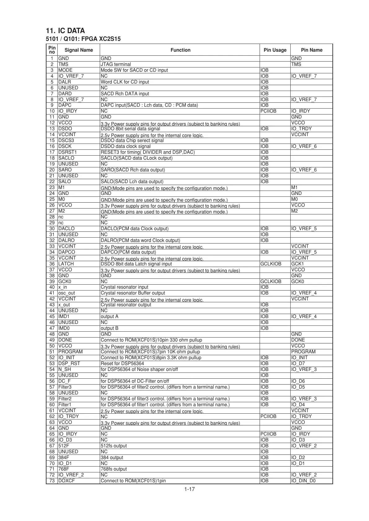
11. IC DATA
Pin
no
Signal Name Function Pin Usage Pin Name
1 GND GND GND
2 TMS JTAG terminal TMS
3 MODE Mode SW for SACD or CD input IOB
4 IO_VREF_7 NC IOB IO_VREF_7
5 DALR Word CLK for CD input IOB
6 UNUSED NC IOB
7 DARD SACD Rch DATA input IOB
8 IO_VREF_7 NC IOB IO_VREF_7
9 DAPC DAPC input(SACD : Lch data, CD : PCM data) IOB
10 IO_IRDY NC PCIIOB IO_IRDY
11 GND GND GND
12 VCCO
3.3v Power su
VCCO
13 DSDO DSDO 8bit serial data signal IOB IO_TRDY
14 VCCINT
2.5v Power su
ins for the internal core lo
ic.
VCCINT
15 DSCS3 DSDO data Chip serect signal IOB
16 DSCK DSDO data clock signal IOB IO_VREF_6
17 DSRST1 RESET3 for timing( DIVIDER and DSP,DAC) IOB
18 SACLO SACLO(SACD data CLock output) IOB
19 UNUSED NC IOB
20 SARO SARO(SACD Rch data output) IOB IO_VREF_6
21 UNUSED NC IOB
22 SALO SALO(SACD Lch data output) IOB
23 M1
GND
M1
24 GND GND GND
25 M0
GND
M2
28 nc NC
29 nc NC
30 DACLO DACLO(PCM data Clock output) IOB IO_VREF_5
31 UNUSED NC IOB
32 DALRO DALRO(PCM data word Clock output) IOB
33 VCCINT
2.5v Power su
ins for the internal core lo
ic.
VCCINT
34 DAPCO DAPCO(PCM data output) IOB IO_VREF_5
35 VCCINT
2.5v Power su
ins for the internal core lo
ic.
VCCINT
36 LATCH DSDO 8bit data Latch signal input GCLKIOB GCK1
37 VCCO
3.3v Power su
VCCO
38 GND GND GND
39 GCK0 NC GCLKIOB GCK0
40 x_in Crystal resonator input IOB
41 osc_out Crystal resonator Buffer output IOB IO_VREF_4
42 VCCINT
2.5v Power su
ins for the internal core lo
ic.
VCCINT
43 x_out Crystal resonator output IOB
44 UNUSED NC IOB
45 IMD1 output A IOB IO_VREF_4
46 UNUSED NC IOB
47 IMD0 output B IOB
48 GND GND GND
49 DONE Connect to ROM(XCF01S)10pin 330 ohm pullup DONE
50 VCCO
3.3v Power su
VCCO
51 PROGRAM Connect to ROM(XCF01S)7pin 10K ohm pullup PROGRAM
52 IO_INIT Connect to ROM(XCF01S)8pin 3.3K ohm pullup IOB IO_INIT
53 DSP_RST Reset for DSP56364 IOB IO_D7
54 N_SH for DSP56364 of Noise shaper on/off IOB IO_VREF_3
55 UNUSED
NC
IOB
56 DC_F for DSP56364 of DC-Filter on/off IOB IO_D6
57 Filter3 for DSP56364 of filter2 control. (differs from a terminal name.) IOB IO_D5
58 UNUSED
NC
IOB
59 Filter2 for DSP56364 of filter3 control. (differs from a terminal name.) IOB IO_VREF_3
60 Filter1 for DSP56364 of filter1 control. (differs from a terminal name.) IOB IO_D4
61 VCCINT
2.5v Power su
ins for the internal core lo
ic.
VCCINT
62 IO_TRDY
NC
PCIIOB IO_TRDY
63 VCCO
3.3v Power su
VCCO
64 GND GND GND
65 IO_IRDY NC PCIIOB IO_IRDY
66 IO_D3 NC IOB IO_D3
67 512F 512fs output IOB IO_VREF_2
68 UNUSED NC IOB
69 384F 384 output IOB IO_D2
70 IO_D1 NC IOB IO_D1
71 768F 768fs output IOB
72 IO_VREF_2 NC IOB IO_VREF_2
73 DOXCF Connect to ROM(XCF01S)1pin IOB IO_DIN_D0
5101 / Q101: FPGA XC2S15
All manuals and user guides at all-guides.com


 To Next Page