49 50
No. Pin Name I/O Function
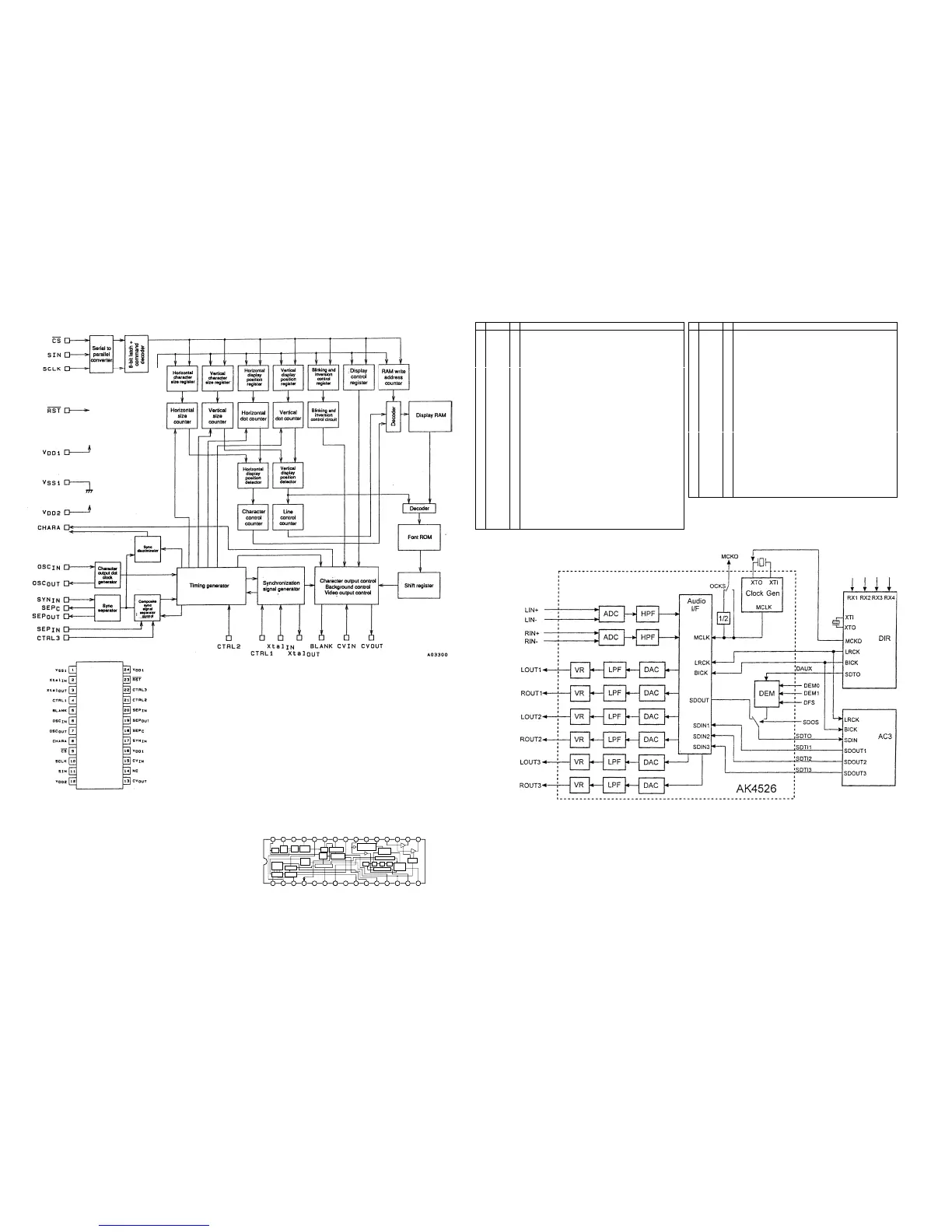
1 SDOS I SDTO Source Select Pin
L: Internal ADC output, "H": DAUX input
Ored with serial control register if P/S="L".
2 OCKS I MCKO Clock Frequency Select Pin
L: MCLK, "H" MCLK12 ORed with serial control register if P/S "L"
3 M/S I Audio Data Master/Slave Mode Select Pin
L: Slave mode. "H": Master mode
4 BICK I/O Audio Serial Data Clock Pin
5 LRCK l/O Input/Output Channel Clock Pin
6 SDTI1 I DAC1 Audio Serial Data Input Pin
7 SDTI2 I DAC2 Audio Serial Data Input Pin
8 SDTI3 I DAC3 Audio Serial Data Input Pin
9 SDTO O Audio Serial Data Output Pin
10 DAUX I AUX Audio Serial Data Input Pin
11 DFS I Double Speed Sampling Mode Pin
"L": Normal Speed, "H": Double Speed, the ADC is powered down.
Ored with serial control register if P/S="L".
12 DEM1 I De-emphasis Pin
Ored with serial control register if P/S="L"
13 DEM0 I De-emphasis Pin
Ored with serial control register if P/S="L"
14 MCKO O Master Clock Output Pin
15 DVDD Digital Power Supply Pin
16 DVSS Digital Ground Pin
17 PD I Power-Down & Reset Pin
When "L", the AK4526 is powered-down and the control registers are reset
to default state. If the state of P/S, M/S, CAD0-1 changes, then the AK4526
must be reset by PD.
18 XTS I X'tal oscillator Select/Test Mode Pin
H: X'tal Oscillator selected
L: External clock source selected
19 ICKS1 I Input Clock Select 1 Pin
20 ICKS0 I Input Clock Select 0 Pin
21 CAD1 I Chip Address Pin
Used during the serial control mode
22 CAD0 l Chip Address Pin
Used during the serial control mode.
No. Pin Narne I/O Function
23 LOUT3 O Lch #3 analog output pin
24 ROUT3 O Rch #3 analog output pin
25 LOUT2 O Lch #2 analog output pin
26 ROUT2 O Rch #2 analog output pin
27 LOUT1 O Lch #1 analog output pin
28 ROUT1 O Rch #1 analog output pin
29 LIN- I Lch Analog Negative Input Pin
30 LIN+ I Lch Analog Positive Input pin
31 RlN- I Rch Analog Negative Input Pin
32 RIN+ I Rch Analog Positive Input pin
33 VREFL l Negative Voltage Reference Input Pin, AVSS
34 VCOM O Common Voltage Output Pin, AVDD/2
Large external capacitor is used to reduce power-supply noise
35 VREPH l Positive Voltage Reference Input Pin, AVDD
36 AVDD Analog Power Supply Pin
37 AVSS Analog Ground pin
38 XTI l X'tal Input Pin
39 XTO O X'tal Output Pin if XTS="H"
MCKI I External Master Clock Input Pin if XTS="L"
40 P/S I Parallel Serial Select Pin
L: Serial control mode, "H": Parallel control mode
41 DIP0 I Audio Data Interface Format Pin in parallel mode
CS I Chip Select Pin in serial mode
42 DIF1 I Audio Data Interface Format Pin in parallel mode
CCLK I Control Data Clock Pin in serial mode
43 LOOP0 l Loop-back Mode Pin in parallel mode
I Enables digital loop-bock from ADC to 3 DACs
CDTI Control Data Input Pin in serial mode
44 LOOP1 I Loop-back Mode Pin in parallel mode
Enables all 3 DAC channels to be input fgrom SDTI1
CDTO O Control Data Output Pin in serial mode
If pins XTS, ICKS0, ICKS1, PD, P/S, DFS, DEM0, DEM1, CAD0, CAD1,
M/S, OCKS, SDOS are not driven then XTS, ICKS0, ICKS1, CAD0, CAD1
must be tied to either AVSS or AVDD, PD, P/S, DPS, DEM0, DEM1, M/S,
OCKS, SDOS must be tied to either DVSS or DVDD
QK04:AK4526
QL04,QL62,QX06:LC74781
Q201:LA1837
1 2 3 4 5 6 7 8 9 10 11 12 13 14 15
161718192021222324252627282930
VCCGND
FM IF
REG
AM
OSC
AM
MIX
AM
RF AMP
AGC
AM/FM
BUFF
IF/DET
AM
COMP
BUFF
DECORDER
MUTE
STEREO
SW
PILOT
DET
FF
FF
FF
VCO
V-S M
AM
S-METER
STEREO DRV.
PHASE DET
SD
TUNING DRIVE
FM DET
S-CURVE
FM
S-METER
L
R
L
R
Q201 LA1837