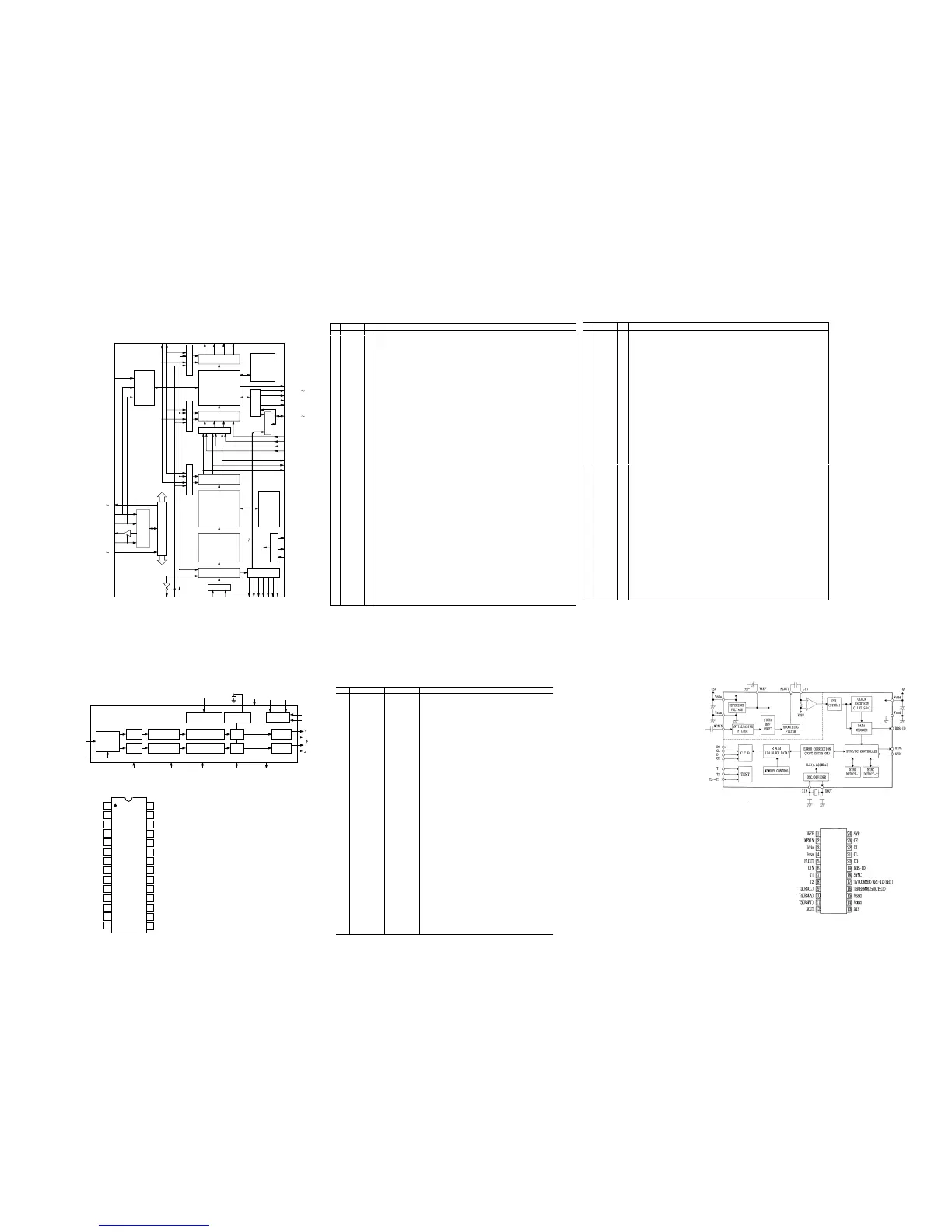
QD01:AD1855
47 48
Pin Input/Output Pin Name Description
1 I DGND Digital Ground.
2 I MCLK Master Clock Input. Connect to an external clock source at either 256, 384
or 512 F
S
.
3 I CLATCH Latch input for control data. This input is rising-edge sensitive.
4 I CCLK Control clock input for control data. Control input data must be valid on the
rising edge of CCLK. CCLK may be continuous or gated.
5 I CDATA Serial control input, MSB first, containing 16 bits of unsigned data per
channel. Used for specifying channel specific attenuation and mute.
6 I 384/256 Selects the master clock mode as either 384 times the intended sample fre-
quency (HI) or 256 times the intended sample frequency (LO). The state of
this input should be hardwired to logic HI or logic LO, or may be changed
while the AD1855 is in power-down/reset. It must not be changed while the
AD1855 is operational.
7 I X2MCLK Selects internal clock doubler (LO) or internal clock = MCLK (HI).
8 O ZEROR Right Channel Zero Flag Output. This pin goes HI when Right Channel has
no signal input for more than 1024 LR Clock Cycles.
9 I DEEMP De-Emphasis. Digital de-emphasis is enabled when this input signal is HI.
This is used to impose a 50 ms/15 m
s response characteristic on the output
audio spectrum at an assumed 44.1 kHz sample rate.
10 I
96/48
Selects 48 kHz (LO) or 96 kHz Sample Frequency Control.
11, 15 I AGND Analog Ground.
12 O OUTR+ Right Channel Positive line level analog output.
13 O OUTRÐ Right Channel Negative line level analog output.
14 O FILTR Voltage Reference Filter Capacitor Connection. Bypass and decouple the
voltage reference with parallel 10
m F and 0.1 mF capacitors to the AGND.
16 O OUTLÐ Left Channel Negative line level analog output.
17 O OUTL+ Left Channel Positive line level analog output.
18 I AVDD Analog Power Supply. Connect to analog +5 V supply.
19 O FILTB Filter Capacitor connection, connect 10 m
F capacitor to AGND.
20 I IDPM1
Input serial data port mode control one. With IDPM0, defines one of four
serial modes.
21 I IDPM0 Input serial data port mode control zero. With IDPM1, defines one of four
serial modes.
22 O ZEROL Left Channel Zero Flag output. This pin goes HI when Left Channel has no
signal input for more than 1024 LR Clock Cycles.
23 I MUTE Mute. Assert HI to mute both stereo analog outputs. Deassert LO for nor-
mal operation.
24 I PD/RST Power-Down/Reset. The AD1855 is placed in a low power consumption
mode when this pin is held LO. The AD1855 is reset on the rising edge of
this signal. The serial control port registers are reset to the default values.
Connect HI for normal operation.
25 I L/RCLK Left/ Right clock input for input data. Must run continuously.
26 I BCLK Bit clock input for input data. Need not run continuously; may be gated or
used in a burst fashion.
27 I SDATA Serial input, MSB first, containing two channels of 16, 18, 20, and 24 bits of
twos complement data per channel.
28 I DVDD Digital Power Supply Connect to digital +5 V supply.
TOP VIEW
(Not to Scale)
28
27
26
25
24
23
22
21
20
19
18
17
16
15
1
2
3
4
5
6
7
8
9
10
11
12
13
14
AD1855
FILTR
OUTRÐ
OUTR+
AGND
96/48
DEEMP
ZEROR
DGND
MCLK
CLATCH
CCLK
X2MCLK
384/256
CDATA
AGND
OUTLÐ
OUTL+
AVDD
FILTB
IDPM1
IDPM0
DVDD
SDATA
BCLK
L/RCLK
ZEROL
MUTE
PD/RST
ATTEN/
MUTE
ATTEN/
MUTE
SERIAL
DATA
INTERFACE
83
INTERPOLATOR
MULTIBIT SIGMA-
DELTA MODULATOR
SERIAL CONTROL
INTERFACE
CLOCK
CIRCUIT
OUTPUT
BUFFER
OUTPUT
BUFFER
DAC
DAC
MULTIBIT SIGMA-
DELTA MODULATOR
VOLTAGE
REFERENCE
VOLUME
MUTE
CONTROL DATA
INPUT
3
2
DIGITAL
SUPPLY
CLOCK
IN
96/48F
S
CLOCK
ANALOG
OUTPUTS
22
ZERO
FLAG
ANALOG
SUPPLY
DE-EMPHASISMUTE
PD/RST
2
SERIAL
MODE
16-/18-/20-/24-BIT
DIGITAL
DATA INPUT
AD1855
83
INTERPOLATOR
3
384/256
X2MCLK
6. IC DATA
CPO
XO
XI
SDOB0
SDOB1
SDOB2
SDWCK1
SDBCK1
OPORT0 7
IPORT0
7
SO
SI
SCK
/CS
OVFB
RAMA0
16
RAMOEN
RAMWEN
RAMCEN
RAMD0
7
SDIB2
SDIB1
SDIB0
SDOA2
SDOA1
SDOA0
Delay RAM
SDIASEL
SDIA1
SDIA0
SDWCK0
SDBCK0
/SDBCK0
/CSB
SCK
SI
SDOACKSEL SDIBCKSEL
SDOBCKSEL
Operating clock
(30MHz)
CRC
ERAMUSE
SDOB Interface
24 * 16
Sub DSP
SDIB Interface
SDOA Interface
SDIBSEL
SDIA Interface
24 * 24
Main DSP
AC-3/Pro Logic/DTS
Data RAM
ExternalRAM
Interface
Coefficient /
Program RAM
STREAM 0
7
PLL
L, R
LS, RS
C, LFE
SDOB3
SDIB3
SURENC
KARAOKE
MUTE
CRC
AC3DATA
DTSDATA
NONPCM
Input Buffer
Decoder
Microprocessor
Interface
Control Registers
Control signals
Control signals
No. NAME I/O FUNCTION
1 VDD1 - +5V power supply (for I/Os)
2 RAMCEN O External SRAM Interface /CE
3 RAMA16 O External SRAM Interface address 16
4 RAMA15 O External SRAM Interface address 15
5 SDIB0 I+ PCM input 0 to Sub DSP
6 SDIB1 I+ PCM input 1 to Sub DSP
7 SDIB2 I+ PCM input 2 to Sub DSP
8 XI I Crystal oscillator connection or input external clock (12.288 MHz)
9 XO o Crystal oscillator connection
10 VSS - Ground
11 AVDD - +3.3V power supply (for PLL circuit)
12 SDIB3 I+ PCM input 3 to Sub DSP
13 TEST Test terminal (to be open in normal use)
14 TEST Test terminal (to be open in normal use)
15 OVFB O Detection of overflow at Sub DSP
16 DTSDATA O DTS data detection (Refer to "Status Register".)
17 AC3DATA O AC-3 data detection (Refer to "Status Register" .)
18 SDOB3 O PCM output from Sub DSP
19 CPO A Output terminal for PLL, to be connected to ground through the external analog filter circuit.
(Refer to "External Circuit for PLL" .)
20 AVSS - Ground (for PLL circuit)
21 VDD2 - +3.3V power supply (for core logic)
22 SDOA2 o PCM output from Main DSP (C, LFE)
23 SDOA1 O PCM output from Main DSP (LS, RS)
24 SDOA0 O PCM output from Main DSP (L, R)
25 RAMA14 O External SRAM Interface address 14
26 RAMA13 O External SRAM Interface address 13
27 RAMA12 O External SRAM Interface address 12
28 RAMA11 O External SRAM Interface address 11
29 RAMA10 O External SRAM Interface address 10
30 VSS - Ground
31 VDD1 - +5V power supply (for I/Os)
32 OPORT0 O Output port for general purpose. (Refer to " OPORT Register")
33 OPORT1 O Output port for general purpose. (Refer to " OPORT Register")
34 OPORT2 O Output port for general purpose. (Refer to " OPORT Register")
35 OPORT3 O Output port for general purpose. (Refer to " OPORT Register")
36 OPORT4 O Output port for general purpose. (Refer to " OPORT Register")
37 OPORT5 O Output port for general purpose. (Refer to " OPORT Register")
38 OPORT6 O Output port for general purpose. (Refer to " OPORT Register")
39 OPORT7 O Output port for general purpose. (Refer to " OPORT Register")
40 VSS - Ground
41 VDD2 - +3.3V power supply (for core logic)
42 RAMA9 O External SRAM interface address 9
43 RAMA8 O External SRAM interface address 8
44 RAMA7 O External SRAM interface address 7
45 SDOB2 O PCM output from Sub DSP
46 SDOB1 O PCM output from Sub DSP
47 SDOB0 O PCM output from Sub DSP
48 SDBCK1 I+ Bit clock input for SDOA, SDIB, SDOB. (Refer to " SDOA, SDIB, SDOB Register")
49 SDWCK1 I+ Word clock input for SDOA, SDIB, SDOB. (Refer to " SDOA, SDIB, SDOB Register")
50 VSS - Ground
No. NAME I/O FUNCTION
51 VDD2 - +3.3V power supply (for core logic)
52 NONPCM O Detection of non PCM data. (Refer to " Status Register")
53 CRC O Detection of AC-3 CRC error. (Refer to " Status Register")
54 MUTE O Detection of auto-mute. (Refer to " Status Register")
55 KARAOKE O Detection of AC-3 karaoke data. (Refer to " Status Register")
56 SURENC O Detection of AC-3 2/0 mode Dolby surround encoded input (Refer to " Status Register")
57 /SDBCK0 O Inverted SDBCKO clock output (refer to " Block diagram")
58 RAMA6 O External SRAM Interface address 6
59 RAMA5 O External SRAM Interface address 5
60 VSS - Ground
61 RAMA4 O External SRAM Interface address 4
62 /lC Is Initial clear
63 TEST Test terminal (to be open in normal use)
64 RAMA3 O External SRAM Interface address 3
65 /CSB Is+ Sub DSP Chip select
66 /CS Is Microprocessor interface Chip select
67 SO Ot Microprocessor interface Serial data output
68 SI Is Microprocessor interface/Sub DSP Serial data input
69 SCK Is Microprocessor interface/Sub DSP clock input
70 RAMA2 O External SRAM Interface address 2
71 VDD1 - +5V power supply (for I/Os)
72 RAMD0 I+/O External SRAM Interface data (STREAM 0 output when External SRAM is not in use)
73 RAMD1 I+/O External SRAM Interface data (STREAM 1 output when External SRAM is not in use)
74 RAMD2 I+/O External SRAM Interface data (STREAM 2 output when External SRAM is not in use)
75 RAMD3 I+/O External SRAM Interface data (STREAM 3 output when External SRAM is not in use)
76 RAMD4 I+/O External SRAM Interface data (STREAM 4 output when External SRAM is not in use)
77 RAMD5 I+/O External SRAM Interface data (STREAM 5 output when External SRAM is not in use)
78 RAMD6 I+/O External SRAM Interface data (STREAM 6 output when External SRAM is not in use)
79 RAMD7 I+/O External SRAM Interface data (STREAM 7 output when External SRAM is not in use)
80 VSS - Ground
81 VDD2 - +3.3V power supply (for core logic)
82 SDWCK0 I Word clock input for SDIA, SDOA, SDIB, SDOB (Refer to " SDIA, SDOA, SDIB, SDOB Register")
83 SDBCK0 I Bit clock input for SDIA SDOA SDIB SDOB (Refer to " SDIA, SDOA, SDIB, SDOB Register")
84 SDIA0 I AC-3/DTS bitstream (or PCM) data input for Main DSP (Refer to " SDIA Register")
85 SDIA1 I AC-3/DTS bitstream (or PCM) data input for Main DSP (Refer to " SDIA Register")
86 RAMA1 O External SRAM Interface address 1
87 RAMA0 O External SRAM Interface address 0
88 RAMWEN O External SRAM Interface /WE
89 RAMOEN O External SRAM Interface /OE
90 VSS - Ground
91 VDD2 - +3.3V power supply (for core logic)
92 IPORT7 I+ Input port for general purpose (Refer to " IPORT Register")
93 IPORT6 I+ Input port for general purpose (Refer to " IPORT Register")
94 IPORT5 I+ Input port for general purpose (Refer to " IPORT Register")
95 IPORT4 I+ Input port for general purpose (Refer to " IPORT Register")
96 IPORT3 I+ Input port for general purpose (Refer to " IPORT Register")
97 IPORT2 I+ Input port for general purpose (Refer to " IPORT Register")
98 IPORT1 I+ Input port for general purpose (Refer to " IPORT Register")
99 IPORT0 I+ Input port for general purpose (Refer to " IPORT Register")
100 VSS Ground
Note ) Is : Schmidt trigger input terminal
I+ : Input terminal with a pull-up resistor
O : Digital output terminal
Ot : Tri-state digital output terminal
A : Analog terminal
Q601:YSS912
Q351:LC72722