Doc. No. MV-S105540-00, Rev. A
Document Classification: Proprietary Information Page 19
Signal Description
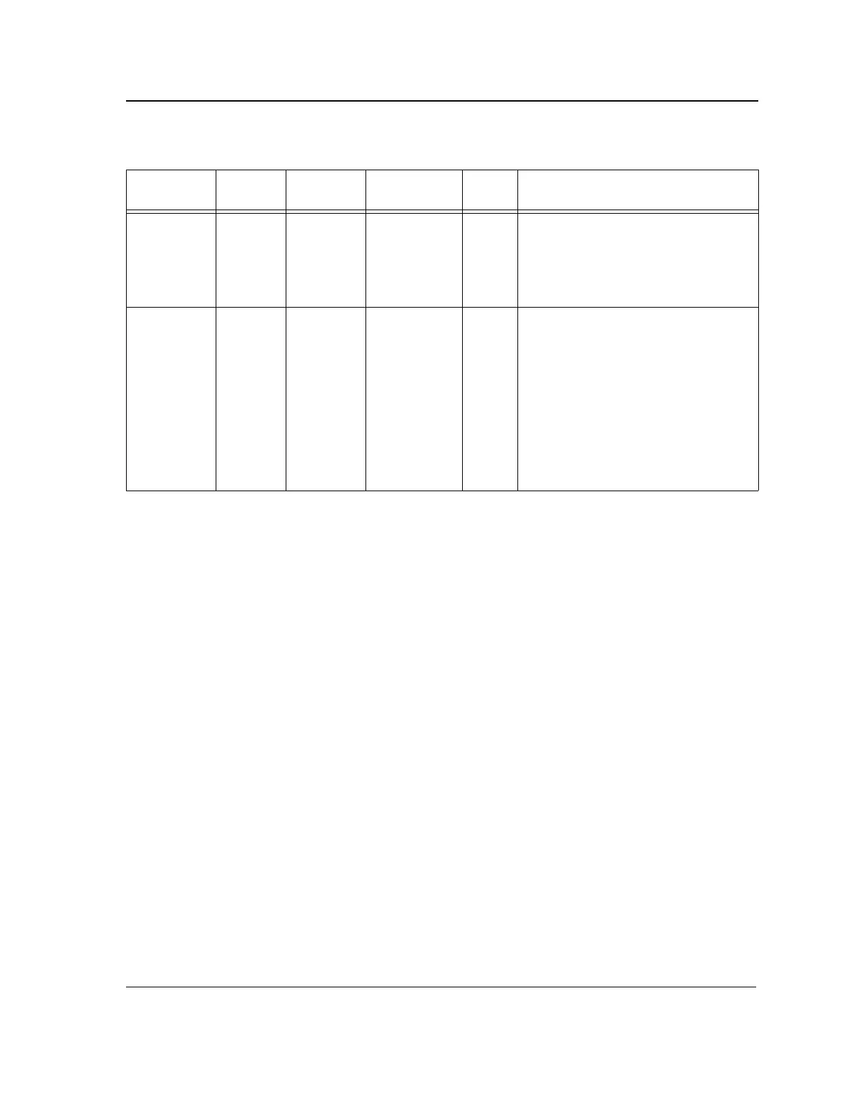
Pin Description
B1 B44 4 RX_DV/
RX_CTL
O, Z RGMII Receive Control. In RGMII mode,
RX_DV is used as RX_CTL. RX_DV is pre-
sented on the rising edge of RX_CLK.
A logical derivative of RX_DV and RX_ER is
presented on the falling edge of RX_CLK.
B3
C3
D3
B2
A49
A50
B43
A51
125
126
128
3
RXD[3]/RD[3]
RXD[2]/RD[2]
RXD[1]/RD[1]
RXD[0]/RD[0]
O, Z RGMII Receive Data. In RGMII mode,
RXD[3:0] are used as RD[3:0]. In RGMII
mode, RXD[3:0] run at double data rate with
bits [3:0] presented on the rising edge of
RX_CLK, and bits [7:4] presented on the fall-
ing edge of RX_CLK. In this mode, RXD[7:4]
are ignored.
In RGMII 10/100BASE-T modes, the receive
data nibble is presented on RXD[3:0] on the
rising edge of RX_CLK.
RXD[3:0] are synchronous to RX_CLK.
Table 4: RGMII Interface (Continued)
117-TFBGA
Pin #
96-aQFN
Pin #
128-PQFP
Pin #
Pin Name Pin
Type
Description
Copyright © 2020 Marvell
December 2, 2020
 Loading...