SLM770A Module Hardware Design Manual
MeiG Smart Technology Co., Ltd 77/77
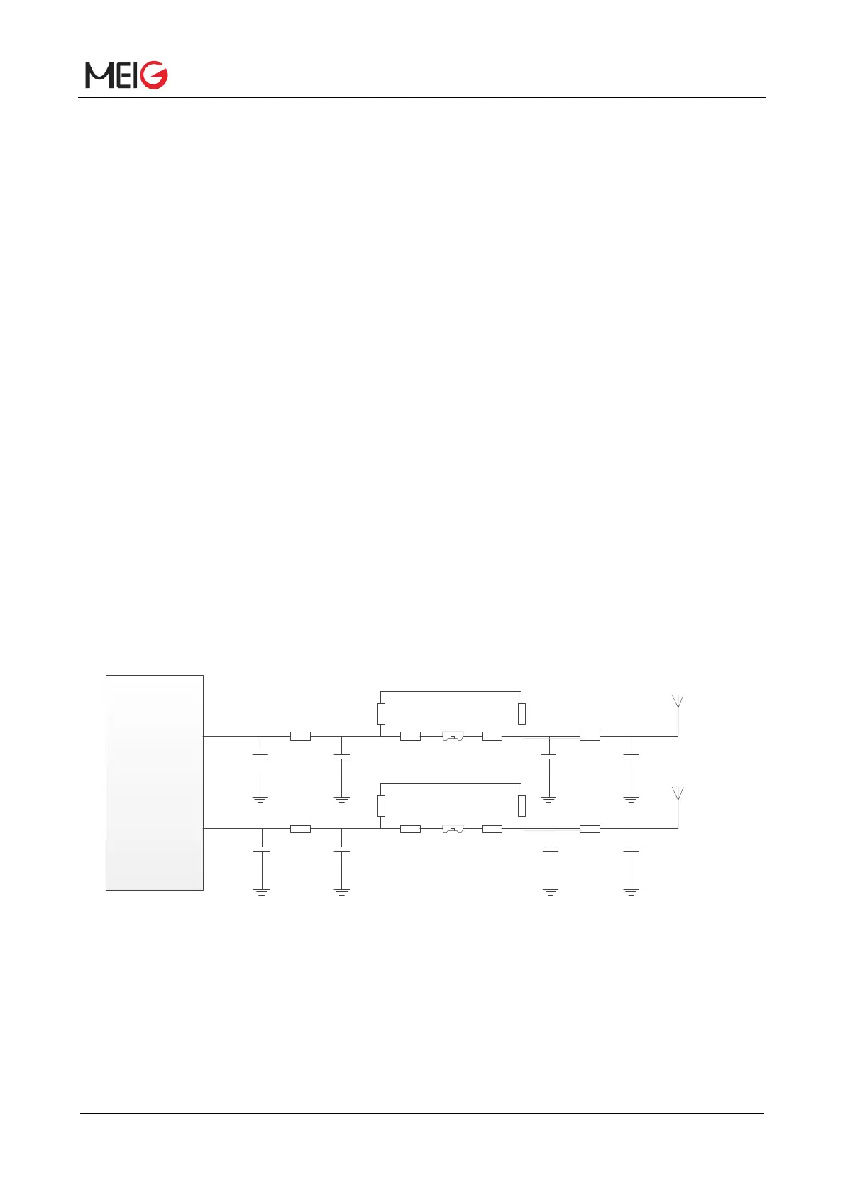
5.2 RF Reference Circuit
ANT_MAIN and ANT_DIV antenna connection is shown in the figure below. In order to obtain better RF
performance, pay attention to the following four points in schematic diagram design and PCB layout:
1. In schematic diagram design, reserve π-type matching circuit near the RF port of the module, and
the capacitor is not attached by default;
2. In schematic diagram design, provide redundant RF connector from the module RF port to an
antenna, used for certification testing, the RF connector may not be attached after mass production and
delivery (Reference: RF connector-1P-H176);
3. In schematic diagram design, reserve π-type matching circuit near the antenna and the capacitor is
not attached by default;
4. In PCB layout, the routing from the module RF port to an antenna is as short as possible, and the
board factory shall make 50Ω impedance control on RF routing PCB layout;
Note: Customers need to consider the impedance matching between backplane and module. The
reserved matching should be optimized according to the actual situation to ensure the optimum
performance.
 Loading...