dsPIC33/PIC24 Family Reference Manual
DS30009740B-page 18 2010-2013 Microchip Technology Inc.
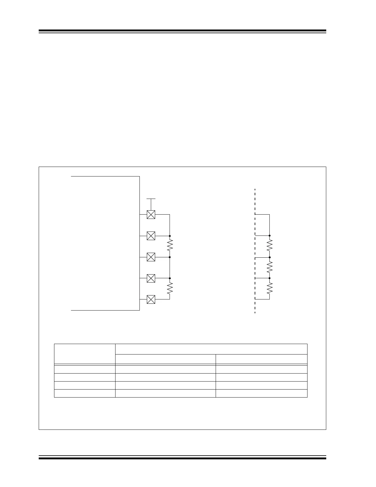
5.3.3 M2 (RESISTOR LADDER WITH SOFTWARE CONTRAST)
M2 operation also uses the LCD regulator but disables the charge pump. The regulator’s internal
voltage reference remains active as a way to regulate contrast. It is used in cases where the
current requirements of the LCD exceed the capacity of the regulator’s charge pump.
In this configuration, the LCD Bias voltage levels are created by an external resistor voltage
divider, connected across LCDBIAS0 through LCDBIAS3, with the top of the divider tied to V
DD
(Figure 5-5). The potential at the bottom of the ladder is determined by the LCD regulator’s volt-
age reference, tied internally to LCDBIAS0. The Bias type is determined by the voltages on the
LCDBIAS pins, which are controlled by the configuration of the resistor ladder. Most applications
using M2 will use a 1/3 or 1/2 Bias type. While Static Bias can also be used, it offers extremely
limited contrast range and additional current consumption over other Bias Generation modes.
Like M1, the LCDBIAS bits can be used to control contrast, limited by the level of V
DD supplied
to the device. Also, since there is no capacitor required across V
LCAP1 and VLCAP2, these pins
are available as digital I/O ports: RG2 and RG3. M2 is selected by clearing the CKSEL<1:0> bits
and setting the CPEN bit.
Figure 5-5: Resistor Ladder Connections for M2 Configuration
LCDBIAS3
Note 1: These values are provided for design guidance only. They should be optimized for the application by the
designer based on the actual LCD specifications.
Bias Level at Pin
Bias Type
1/2 Bias 1/3 Bias
LCDBIAS0 (Internal Low Reference Voltage) (Internal Low Reference Voltage)
LCDBIAS1 1/2 V
BIAS 1/3 VBIAS
LCDBIAS2 1/2 VBIAS 2/3 VBIAS
LCDBIAS3 VBIAS (up to AVDD)VBIAS (up to AVDD)
10 k
(1)
10 k
(1)
1/2 Bias 1/3 Bias
LCDBIAS2
LCDBIAS1
LCDBIAS0
AV
DD
10 k
(1)
10 k
(1)
10 k
(1)
VDD
dsPIC33/PIC24