dsPIC33/PIC24 Family Reference Manual
DS30009740B-page 20 2010-2013 Microchip Technology Inc.
5.4 Design Considerations for the LCD Charge Pump
When designing applications that use the LCD regulator with the charge pump enabled, users
must always consider both the dynamic current and RMS (Static) current requirements of the dis-
play, and what the charge pump can deliver. Both dynamic and Static current can be determined
by Equation 5-1:
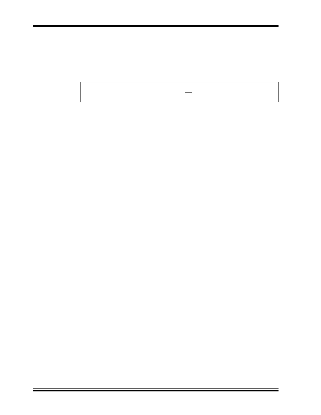
Equation 5-1:
For dynamic current, C is the value of the capacitors attached to LCDBIAS3 and LCDBIAS2. The
variable, dV, is the voltage drop allowed on C2 and C3 during a voltage switch on the LCD
display, and dT is the duration of the transient current after a clock pulse occurs.
For practical design purposes, these will be assumed to be 0.047 ìF for C, 0.1V for dV and 1 ìs
for dT. This yields a dynamic current of 4.7 mA for 1 ìs.
RMS (Root Mean Square) current is determined by the value of C
FLY for C, the voltage across
V
LCAP1 and VLCAP2 for dV, and the regulator clock period (TPER) for dT. Assuming a CFLY value
of 0.047 ìF, a value of 1.02V across C
FLY and a TPER of 30, the maximum theoretical Static cur-
rent will be 1.8 mA. Since the charge pump must charge five capacitors, the maximum current
becomes 360 ìA.
For a real world assumption of 50% efficiency, this yields a practical current of 180 ìA. Users
should compare the calculated current capacity against the requirements of the LCD. While dV
and dT are relatively fixed by device design, the values of C
FLY and the capacitors on the
LCDBIAS pins can be changed to increase or decrease current. As always, any changes should
be evaluated in the actual circuit for their impact on the application.