RS422/RS449/RS485/RS530
TheRS‐422andRS‐485standardsdescribedifferentialelectricalsignalsbutnotconnectororpin
assignments.TheRS‐530andRS‐449standardsdefinespecificconnectorsandpinassignmentsusing
differentialsignals.ThedifferentialsignalsonthecardmeetbothRS‐422andRS‐485electrical
specifications.
RS‐530usesdifferentialsignalsonaDB‐25connector.TheadapterDB‐25connectorfollowsthis
standardwhentheportjumpersareinstalledforRS‐422/485.Useanystraightthrough25conductor
DB‐25MtoDB‐25Fcable(suchasMicroGatePart#CMF000)toconnecttheadaptertoRS‐530
communicationsequipment.
RS‐449usesdifferentialsignalsonaDB‐37connector.TousethisstandardinstalltheRS‐422/485
jumpersfortheportandusetheMicroGateRS‐449cable(Part#2537FM).
ThemaximumdataratesupportedbytheadapterwhenusingRS‐530orRS‐449is10Mbps.Cablelength
andsignalloadingmayreducethemaximumusabledataratefromthisvalue.
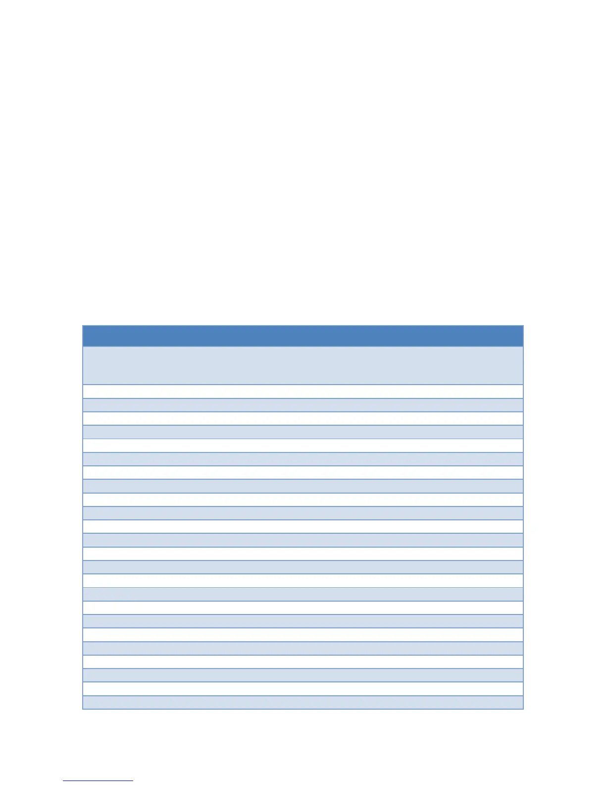
RS‐422/RS‐530/RS‐449MaleDTE
SignalName ElectricalDesc DB25
RS‐530
Pin#
DB37
RS‐449
Pin#
Direction
Earth/ShieldGround 1 1
TxD(+/A),TransmitData RS‐422/V.11 2 4 Output
RxD(+/A),ReceiveData RS‐422/V.11 3 6 Input
RTS(+/A),RequesttoSend RS‐422/V.11 4 7 Output
CTS(+/A),CleartoSend RS‐422/V.11 5 9 Input
DSR(+/A),DataSetReady RS‐422/V.11 6 11 Input
SignalGround 7 19
DCD(+/A),DataCarrierDetect RS‐422/V.11 8 13 Input
RxC(‐/B),ReceiveClock RS‐422/V.11 9 26 Input
DCD(‐/B),DataCarrierDetect RS‐422/V.11 10 31 Input
AuxClk(‐/B),DTEClockOutput RS‐422/V.11 11 35 Output
TxC(‐/B),TransmitClock RS‐422/V.11 12 23 Input
CTS(‐/B),CleartoSend RS‐422/V.11 13 27 Input
TxD(‐/B),TransmitData RS‐422/V.11 14 22 Output
TxC(+/A),TransmitClock RS‐422/V.11 15 5 Input
RxD(‐/B),ReceiveData RS‐422/V.11 16 24 Input
RxC(+/A),ReceiveClock RS‐422/V.11 17 8 Input
LL,LocalLoopbackControl RS‐232/V.28 18 10 Output
RTS(‐/B),RequesttoSend RS‐422/V.11 19 25 Output
DTR(+/A),DataTerminalReady RS‐422/V.11 20 12 Output
RL,RemoteLoopbackControl RS‐232/V.28 21 14 Output
DSR(‐/B),DataSetReady RS‐422/V.11 22 29 Input
DTR(‐/B),DataTerminalReady RS‐422/V.11 23 30 Output
AuxClk(+/A),DTEClockOutput RS‐422/V.11 24 17 Output