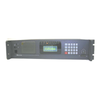
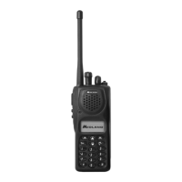
SYN-TECH III P25 PORTABLE RADIO
SERVICE MANUAL
3-2
3.2 Operating Principles
3.2.1 RF and Control PCB
The RF and Control Board is designed to be used in Syn-Tech III P25 Portable Radio. It consists of
Receiver Circuits, Transmitter Circuits, Voltage Controlled Oscillator Circuits, Frequency Synthesizer
Circuits, Control Circuits and Audio Frequency Circuits. The board is supplied by 7.5 V
DC
voltage.
The RF and Control Board carries out receive and transmission functions at the VHF frequency band,
136-174 MHz, the UHF(A) frequency band, 380-470 MHz, or the UHF(B) frequency band, 450-512 MHz.
In receive mode the FM/C4FM modulated RF signal from antenna at selected channel frequency is
decoded. The base band signal is sent to the Keypad and Display Board as audio or data to be
monitored. In transmit mode the base band signal (audio or data) is transformed into an FM modulated
RF signal on selected channel frequency and transmitted to the antenna to be broadcast.
The stand-by mode is used to extend battery life by limiting current. Only the circuits necessary to detect
a signal are active. The circuits operate 5 ms active and 100 ms stand-by in analog mode and 5 ms
active and 25 ms stand-by in digital mode.
3.2.1.1 Receiver Circuits
Receiver circuits have a dual conversion super heterodyne structure. They consist of RF pre input
circuits, first mixer, bi-directional intermediate frequency duplexer, first amplifier of the first intermediate
frequency, 4 pole first intermediate frequency crystal filter, second amplifier of first intermediate
frequency, second mixer, 4 or 6 pole second intermediate frequency ceramic filter, second intermediate
frequency amplifier limiter and FM decoder circuits.
The RF signal from the antenna first passes through the pre input circuits. The RF signal passes through
a low pass harmonic filter, T/R switch and band pass filter or tuned notch filter. The UHF radio’s notch
filter frequency is tuned by the BPF_ADJUST voltage. This 1-4 volt swing tunes the notch from 290-380
MHz.
The RF signal is then amplified about 15 dB by the low noise pre-amplifier and then filtered by a tuned
band pass filter. The 1-4 Volt BPF_TUNE (BPF_ADJUST) adjusts the filter’s center frequency to the
channel frequency, F
chan
.
The 45 MHz first IF frequency is obtained by mixing the RF signal with the first local oscillator signal,
F
chan
-45 MHz. The first IF frequency is filtered amplified and then filtered by the 4 pole crystal filter. The
crystal filter has a 3 dB bandwidth of ±6 KHz. The output of the crystal filter is then amplified by another
first IF amplifier and input to the second mixer within the demodulator IC.
The 450 KHz second IF frequency is obtained by mixing the signal with the 44.550 MHz second local
oscillator signal. The 44.550 MHz second local oscillator signal is obtained as the third harmonic of the
14.85 MHz TCXO. The 450 KHz second IF frequency is filtered by the wide (4 pole, ±7.5 KHz 6 dB
bandwidth) or narrow (6 pole, ±2 KHz 6 dB bandwidth) ceramic filters then sent into the limiter. The
amplifier clipper signal is passed to the fm decoder and the audio + noise signal is output from the
demodulator IC and is sent to an 8 KHz low pass filter to obtain the RX_AUDIO signal and to the noise
filter to get the NOISE_DET_OUT signal.
The NOISE_DET_OUT signal is compared to the SQUELCH_POWER_TUNE (S_G_ADJUST) voltage to
obtain the SQUELCH signal which is sent to the MCU. Additionally, the RSSI signal from the demodulator
IC is sent to the MCU.
3.2.1.2 Transmitter Circuits
The transmitter circuit’s primary function is to amplify the signal from the voltage controlled oscillator, and
transmit it to the antenna between 0.2 W - 5 W output power ranges. The transmitter circuits consist of
driver amplifier, power amplifier, receiver-transmitter switch, harmonic filter and power control units.
The 17-18 dBm level signal from the transmitter VCO is amplified by the driver amplifier, TR502 , then by
the power amplifier , TR501. The signal from the power amplifier is sent to the antenna through the
 Loading...