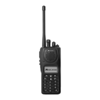
SYN-TECH III P25 PORTABLE RADIO
SERVICE MANUAL
3-4
3.2.1.5 Control Circuits
The control circuits contain the M16C/64 series M62724 microprocessor. The microprocessor has a 384K
byte flash memory. The microprocessor uses 12.288 MHz crystal as clock. It divides this frequency by
two and uses 6.144 MHz as an internal clock. It uses 8 bit data bus structure for external memory access.
There is a 20K byte internal RAM in the microprocessor. A 128K byte external RAM is used as main
RAM. It can be upgraded to 256K byte if it is required. 4M byte EEPROM (Data Flash) is used.
3.2.1.6 Audio Circuits
The audio circuits are composed of mainly the CMX881 integrated circuit. This integrated circuit is a DSP
based mixed signal audio processing circuit. This circuit also processes the CTCSS, DTMF and FFSK
signals. It can run CTCSS and SelCall decode processes synchronously. It requires an 18.432MHz clock
signal. A 6.144MHz signal is generated from the microprocessor. Its 3rd Harmonic is received via filter to
get 18.432MHz clock signal. The CMX881 is a half-duplex integrated circuit, so it can not perform receive
and transmit functions simultaneously. Because the radio is also half-duplex this substructure is sufficient.
The RX_AUDIO signal from the receiver circuits is filtered and de-emphasized within the CMX881. The
output of the CMX881 is the AUDIO signal which is sent to volume control and on to the audio amplifier.
The MIC_AUDIO signal from the microphone element is pre-emphasized within the CMX881. The CM881
also processes the mic audio through the VOGAD circuit, and then the limiter circuit. The mic audio is
sent to the modulator as the TX_AUDIO1 and TX_AUDIO2 signals. The modulation levels and flatness
are adjusted by the tuned amplifiers between the output of the CMX881 and the TX_AUDIO1 and
TX_AUDIO2 signals.
3.2.2 Display and Keypad PCB
The display and keypad board is the user interface for SYN-Tech III P25 Portable Radio. The radio is
controlled by the On/Off-volume knob, channel switch and keypad, which are connected to the board by a
flexible connection. Data and warnings are shown by LEDs and the LCD Display. The radio's connection
to external equipment is achieved via the option connector which is connected to the board by a flexible
connection. In receive mode, the processed audio signal coming from the RF and Control board is
amplified and sent to the speaker. In transmit mode, the audio signal coming from the microphone is
amplified and routed to the RF and Control Board. The RF and Control Board is connected to the Display
and Keypad board by KN2.
3.2.3 DSP PCB
The digital board circuits are controlled by the DSP, TD1. There are two A/D-D/A (Analog/Digital–
Digital/Analog) converter integrated circuits on board. While analog to digital or digital to analog
conversions of audio signals are performed by one of these integrated circuits, analog to digital or digital
to analog conversions of digital modulation signals are performed by the other one. Supply circuits and
circuits that generate a clock signal are also located on the board.
The interface with the microcontroller is through the HPI, which is a special parallel port of the DSP. The
DSP has three synchronous serial ports. The DSP communicates with the baseband Modem A/D–D/A
converter through first serial port, and with the audio A/D –D/A converter through the second serial port.
In the following sections, these interfaces will be explained.
The DSP multiplies the 12.288MHz clock signal by three with the on-chip PLL, so the DSP clock rate
becomes 36.864MHz. For the purpose of power saving, the DSP switches to the stand-by mode while not
operating. The wake up interrupt is sent by the MCU.
3.2.3.1
UDSP–MCU Interface
The DSP is connected to the MCU by connector, KN1 and runs under the control of the MCU. The DSP–
MCU interface is realized through HPI-8 8-bit parallel interface of C54xDSP family. Both the DSP and
MCU can access the RAM area on DSP by HPI-8 interface. There are 8-bit bi-directional data bus and
control signals on interface. The data length used in interface is 16-bit, access is granted at two phases
from 8-bit port based on A0 signal indicating first or second byte. HPI-8 combines the two bytes and then
places it to DSP RAM as 16-bit.

 Loading...