MIMAKI ENGINEERING CO., LTD.
6. Checking damage of the Main PCB ASSY
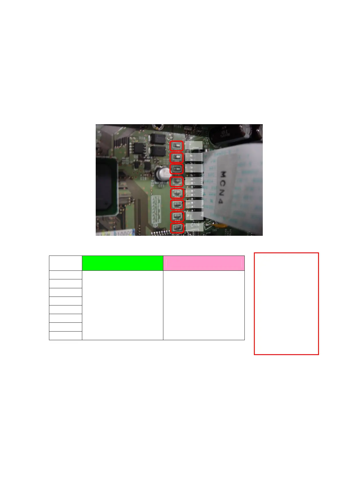
(1) Release the lock located both sides of the connector for HDC_FFC 130/160 ASSY connected to
CN1-CN4 in the Main PCB ASSY and then remove HDC_FFC 130/160 ASSY.
(2) Measure resistance between the test pin TP1-TP8 and GND on the Main PCB ASSY and judge
whether the COM circuit is good or not with List 3.
Connect the Negative terminal of the tester to the GND test pin (GND1-9) and measure the
resistance by getting the Positive terminal touch to TP1-8
In case of the machine which would not be turned on, it is highly possibility of impedance
anomaly of the COM circuit and short circuit between 42V and GND in the Main PCB.
List 3
TP1
TP2
TP3
TP4
TP5
TP6
TP7
TP8
Notes:
If all the measured
value of the TP is
shown in the range
of Abnormal COM
circuit, please
measure that of
normal circuit board
and compare with
them since it may be
variety of the tester.
Test pin
Normal Main PCB COM Abnormal Main PCB COM
TP1
TP2
TP3
TP4
TP5
TP6
TP7
TP8
17K-18KΩ
Good
Less than 17KΩ,
More than 18KΩ
Bad
4/7 D900674 Ver1.1

 Loading...