miniDSP Ltd, Hong Kong / www.minidsp.com / Features and specifications subject to change without prior notice 10
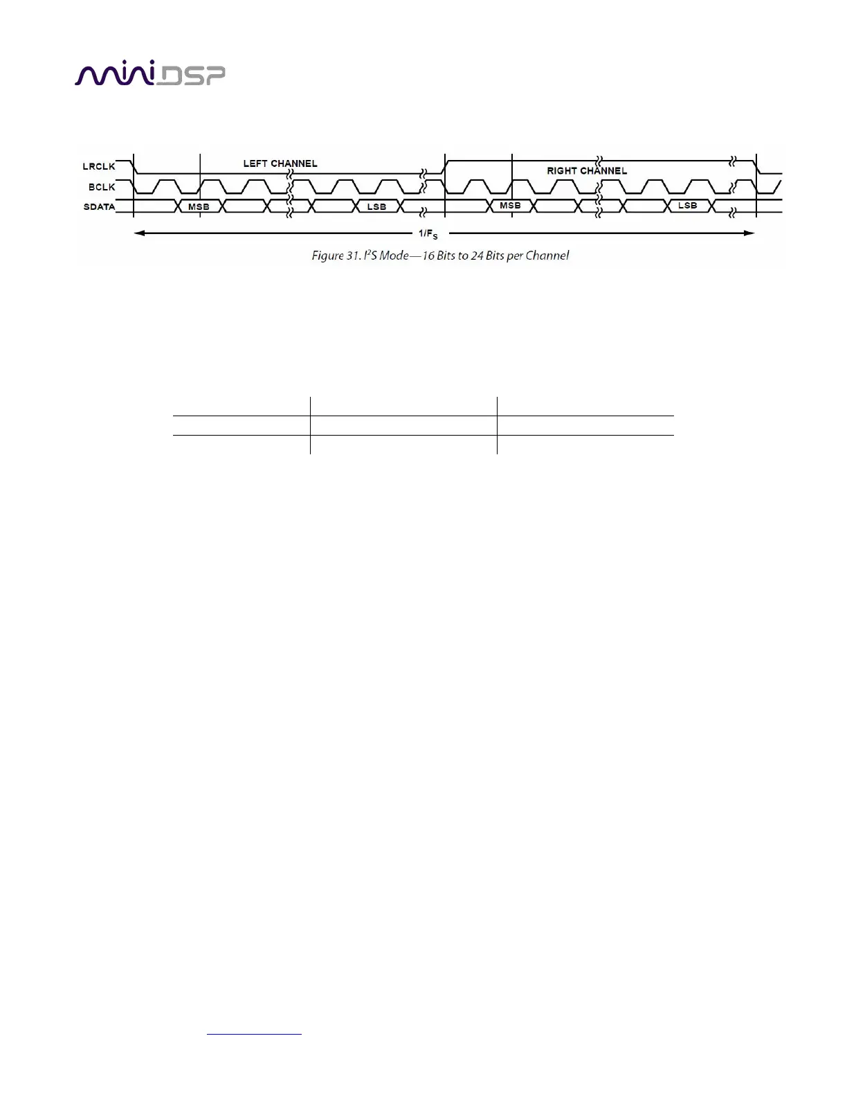
The timing of data lines is determined by the bit clock and the word clock, as illustrated in the following diagram:
The UMA-8 board has four I2S input data lines and four I2S output data lines, each carrying two channels of
audio. Note, however, that current firmware do not make use of all I2S in/out lines. The below table will be
updated over time as we add new features to the firmware.
Table 3. Input and output mapping
The playback output, also called “SPEAKER OUTPUTS” through out this section is to be connected to an external
I2S amplifier or I2S DAC. Feel free to contact miniDSP tech support if you have some specific questions.
2.5 ADDITIONAL I2S USAGE NOTES
Note that I2S is not a “plug and play” protocol. It requires attention to technical details such as clocking and wire
layout. It is a solution for OEMs and advanced DIYers (or professionals) with suitable knowledge, skills and
measurement equipment.
Be sure to take the following precautions when designing your I2S interface and wiring:
General I2S usage notes
• Unbuffered I2S lines must be kept short to ensure clock and data integrity.
• If driving longer lines, buffers may be required for the clock signals (MCLK, LRCLK, and BLCK).
• Observe correct grounding and shielding, and keep analog and digital grounds separated.
• Ensure that the clock ratios (as listed in Table 2) are compatible with connected circuits.
3.3V logic level
All lines use a 3.3V logic level. Ensure that connected circuits use a compatible level (1.8V, for example, will
not work).