2-12 UHF Transmitter (Band 1 and Band 2)
The RF section of the VCOBIC (U3801) is operated at 4.54 V (VSF), while the control section of the
VCOBIC and Fractional-N synthesizer (U3701) is operated at 3.3V. The operation logic is shown in
Table 2-3.
In the receive mode, U3801 pin 19 is low or grounded. This activates the receive VCO by enabling the
receive oscillator and the receive buffer of U3801. The RF signal at U3801 pin 8 is run through a
matching network. The resulting RF signal is the LO RF INJECTION and it is applied to the mixer at
T3302.
During the transmit condition, when PTT is depressed, 3.2 volts is applied to U3801 pin 19. This
activates the transmit VCO by enabling the transmit oscillator and the transmit buffer of U3801. The
RF signal at U3801 pin 10 is injected into the input of the PA module (U3501 pin16). This RF signal is
the TX RF INJECTION. Also in transmit mode, the audio signal to be frequency modulated onto the
carrier is received through U3701 pin 41.
When a high impedance is applied to U3801 pin19, the VCO is operating in BATTERY SAVER mode.
In this case, both the receive and transmit oscillators as well as the receive transmit and prescaler
buffer are turned off.
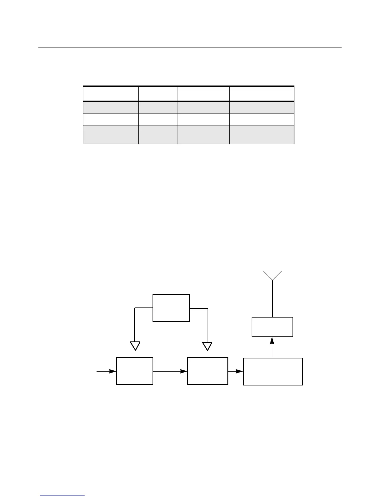
2.6 UHF Transmitter (Band 1 and Band 2)
The UHF transmitter consists of the following basic circuits as shown in Figure 2-10:
• Power Amplifier
• Antenna Switch
• Harmonic Filter
• Antenna Matching Network
• Power Control Integrated Circuit (PCIC).
Table 2-3. VCO Control Logic
Desired Mode AUX 4 AUX 3 TRB
Tx n.u. High (@3.2V) High (@3.2V)
Rx n.u. Low Low
Battery Saver n.u. Hi-Z/Float
(@1.6V)
Hi-Z/Float (@1.6V)
Figure 2-10. Transmitter Block Diagram
PCIC
Antenna
PA
Driver
Vcontrol
Vcontrol
From VCO
Jack
Antenna Switch/
Harmonic Filter/
Matching Network
PA-Final
Stage
 Loading...