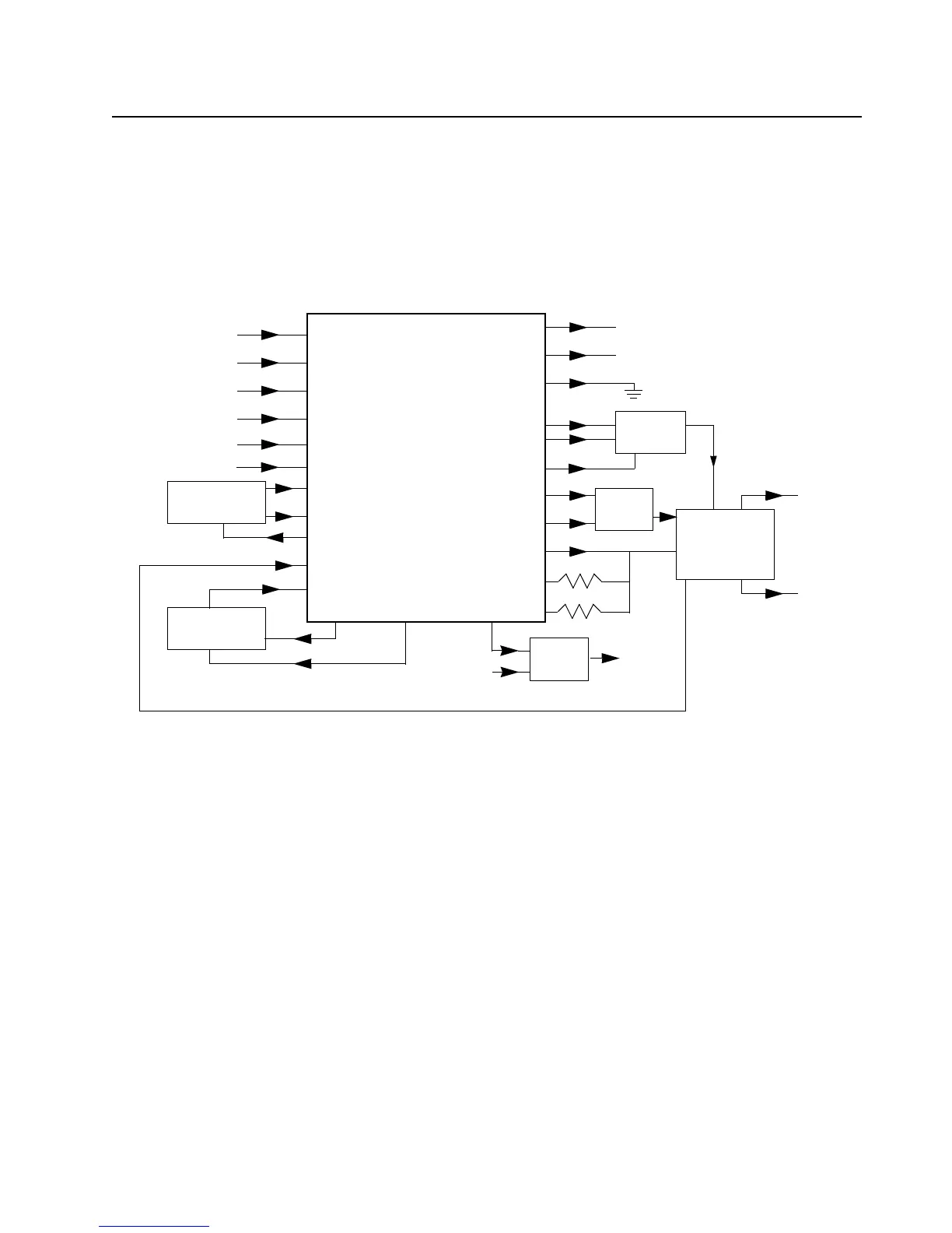
UHF Transmitter (Band 1 and Band 2) 2-17
In achieving fast locking for the synthesizer, an internal adapt charge pump provides higher current at
pin 45 of U201 to put synthesizer within the lock range. The required frequency is then locked by
normal mode charge pump at pin 43.
Both the normal and adapt charge pumps get their supply from the capacitive voltage multiplier which
is made up of C258, C259, C228, triple diode CR201 and level shifters U210 and U211. Two 3.3V
square waves (180 deg out of phase) are first shifted to 5V, then along with regulated 5V, put through
arrays of diodes and capacitors to build up 13.3V at pin 47 of U201.
Figure 2-13. Synthesizer Block Diagram
DATA
CLK
CEX
MODIN
V
CC
, DC5V
XTAL1
XTAL2
WARP
PREIN
VCP
REFERENCE
OSCILLATOR
VOLTAGE
MULTIPLIER
VOLTAGE
CONTROLLED
OSCILLATOR
2-POLE
LOOP
FILTER
DATA (U409 PIN 100)
CLOCK (U409 PIN 1)
CSX (U409 PIN 2)
MOD IN (U404 PIN 40)
+5V (U247 PIN 4)
7
8
9
10
13, 30
23
24
25
32
47
VMULT2 VMULT1
BIAS1
SFOUT
AUX3
AUX4
IADAPT
IOUT
GND
FREFOUT
LOCK
4
19
6, 22, 23, 24
43
45
3
2
28
14
15
40
FILTERED 5V
STEERING
LINE
LOCK (U409 PIN 56)
PRESCALER IN
LO RF INJECTION
TX RF INJECTION
(1ST STAGE OF PA)
FREF (U201 PIN 21 & U404 PIN 34)
39
BIAS2
41
DUAL
TRANSIS
DUAL
TRANSIS-
48
5V
R5
5, 20, 34, 36
(U248 PIN 5)
AUX1
V
DD
, 3.3V
MODOUT
U251
LOW VOLTAGE
FRACTIONAL-N
SYNTHESIZER
TORS
TORS
 Loading...