B-36 | ni.com
Appendix B Timing Diagrams
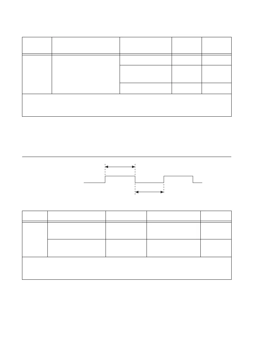
Gate Pulse Width
Figure B-47 and Table B-31 show the timing requirements for Counter n Gate. The requirements
depend on the gating mode.
Figure B-47. Counter n Gate Pulse Width Timing Diagram
Gate to Source Setup and Hold
The counter can be modeled as a set of flip flops where the D input is Count Enable and the clock
input is Selected Source, as shown in Figure B-41. This section shows the setup and hold
requirements for two different cases:
• A PFI pin drives Counter n Source and a different PFI pin drives Counter n Gate
• The general case (all other combinations of signals driving Source and Gate)
t
6
Counter n Source Pulse
Width
80 MHz Source 6.2 —
Other Internal
Source
12.5 —
External Source 16.0 —
*
The times in this table are measured at the pin of the M Series device. For example, t
5
specifies the
minimum period of a signal driving a PFI, RTSI, or PXI_STAR pin when that signal is internally routed
to Counter n Source.
Table B-31. Counter
n Gate Pulse Width Timing
Time Description Gating Mode Min (ns)
*
Max (ns)
t
7
Counter n Gate Pulse
Width
Edge 12.0 —
Counter n Gate Pulse
Width
Level One Source Period —
*
The times in this table are measured at the pin of the M Series device. That is, t
7
specifies the minimum
pulse width of a signal driving a PFI, RTSI, or PXI_STAR pin when that signal is internally routed to
Counter n Gate.
Table B-30. Counter
n Source Timing (Continued)
Time Description
Synchronization
Mode
Min (ns)
*
Max (ns)
 Loading...