B-24 | ni.com
Appendix B Timing Diagrams
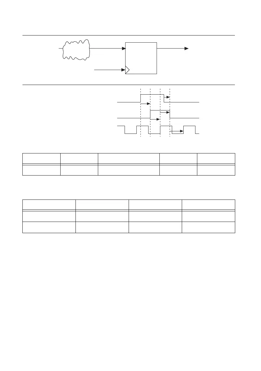
Figure B-28. Pause Trigger Input Delay Path
Figure B-29. Pause Trigger Timing Diagram
Input Timing Verification
Consider an application that uses an external trigger and an external clock. The trigger and clock
signals are routed to an internal D flip-flop (DFF). To ensure that the trigger is sampled on a
particular clock edge, the setup and hold times of the internal DFF must be met:
• Recall that a “terminal” is a PFI pin, RTSI pin, or PXI_Star pin.
• Let TriggerDelay be the delay from the trigger terminal to the DFF.
• Let ClockDelay be the delay from the clock terminal to the DFF.
•Let DFF
Setup
and DFF
Hold
be the setup and hold time of the DFF.
• Let External
Setup
and External
Hold
be the setup and hold time of the trigger to the clock at
the terminals.
Table B-17. Pause Trigger Timing from Signal_i to Selected Pause Trigger
Time From To Min (ns) Max (ns)
t
9
Signal_i Selected Pause Trigger 1.7 7.8
Table B-18. Pause Trigger Setup and Hold Timing
Time Parameter Min (ns) Max (ns)
t
10
Setup 1.5 —
t
11
Hold 0 —
Signal_i
Sync Sample Clock Timebase
DQ To Internal Logic
Logic
Selected Pause
Trigger
Signal_i
Selected Pause Trigger
Sync Sample Clock Timebase
t
9
t
9
t
10
t
11
t
10
 Loading...