then reasserted.
Serial
110
is corltrolled by the RIM and SIM instruction.
SID is read
in by the
RIhl instruction and the SIM instruction sets SOD data.
Name Restart address
(hex) Wherc sensed
TK.4P
241 Level and edge
RST7.5
3c16 Edge
RST6.5
341
6
Level
RST5.5 2c16 Level
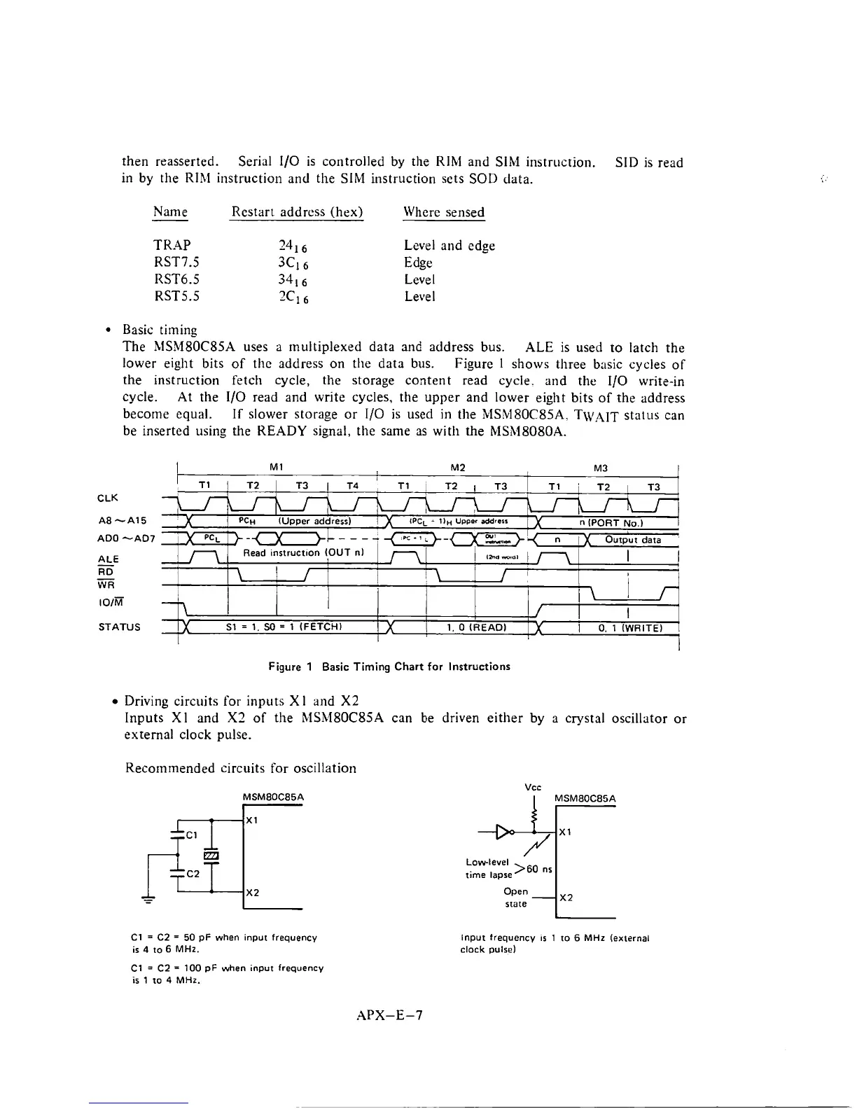
Basic timing
The
hlSM80C85A uses a ~nultiplexed data
and
address bus.
ALE is used
ro
latch the
lower eight bits of
thc address on the data bus.
Figure
1
shows three basic cycles of
the instruction fetch cycle, the storage content read cycle. and the
I/O
write-in
cycle.
At
the
I/O
read and write cycles, the upper and lower eight bits of the address
become
equal. If slower storage or
I/O
is used
in
the hlSM80C85A. Titr~1-r status can
be inserted using the READY signal,
the
same as with
the
MSX18080A.
ADO &AD7
ALE
-
R D
Figure
1
Basic Timing Chart
for
Instructions
-
WR
I
I
o/m
4
i'
\
I
I
Driving circuits for inputs XI and X2
Inputs
XI and
X2
of the MSM80C85A can be driven either by a crystal oscillator or
external clock pulse.
Recommended circuits for oscillation
x
I
0.
1
(WRITE)
1
vcc
I
I
1.
0 (READ)
STATUS
C1
=
C2
=
50
pF when input frequency
is
4
to
6
MHz.
Sl
=
1,
SO
=
1
(FETCH)
IX
Lowlevel
time iapse'60
ns
I
Open state
4
x2
Input frequency
1s
1
to
6
MHz (exirrnal
clock pulse)
C1
=
C2
=
100
pF when input frequency
is
1
to
4
MHz.