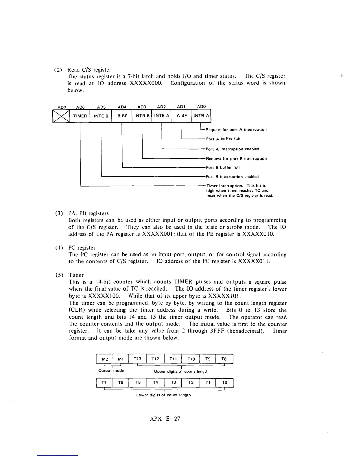
(2)
Read
C/S
register
'I'he status register is a 7-bit latch and holds
1/0
and tirner status.
Thc
C/S
register
is read at
10
address XXXXX000. Configuration of the status word is shown
below.
I I
I
I
Request for port
B
interruption
AD7 AD6 AD5 AD4 AD3 AD2 AD1 ADO
sport
B
buffer full
I
Port
B
interruption enabled
I
T~rner interruption. This bit is
high when timer reaches
TC
and
reset when the
CIS
register is read.
(3)
PA.
PI3
registers
Both
registers
can be used as either input or output ports according to programming
of
the
CIS
register.
They can also be used in the basic or strobe mode.
The
I0
address of the
PA
registcr is XXXXXOOI: that of the
1'B
register is XXXXXO 10.
Request for port
A
interruption
Port
A
buffer full
Port
A
interruption enabled
B
BF
TIMER
(4)
PC
register
The
IJC
register can be used as an input port, output, or for control signal according
to the contents of
CIS
register.
I0
address of the
PC
register is XXXXXOI
I.
INTR
A
INTR
B
INTE
B
(5)
Tirtier
This is a 14-bit counter which counts
TIMER
pulses and outputs a square p~~lse
when the final value
of
TC
is reached. The
I0
address of the timer register's lower
byte
is
XXXXX100.
While that of its upper byte
is
XXXXXlO1.
The timer can be programmed, byte
by
byte. by writing to the count length register
(CLR)
while selecting the timer address during a write. Bits
0
to
13
store the
count length and bits
14 and
I5 the timer output mode.
The operator can read
the counter contents and the output mode. The initial value is first to the counter
register. It can be take any value from
2
through
3FFF
(hexadecimal).
Timer
format and output
mode are shown below.
Output mode
1
Upper digits of count length
INTE
A
I
Lower digits of count length
A
BF