Pin Signal I/O Engine connection Notes
4 V
DD
<- N2200 VSIM2 VSIM2, supply
voltage 1.8
(Max 70mA)
5 CLK <- D4800 MMC2_CLK External clock
for the MMC
card, Max 20
MHz
6 Vss2 GND Ground
7 DAT <-> D4800 MMC2_DAT0 Bi-directional
data bus
- MMCDET -> D4800 btwake1(in)
[P10]
MMC card
detect
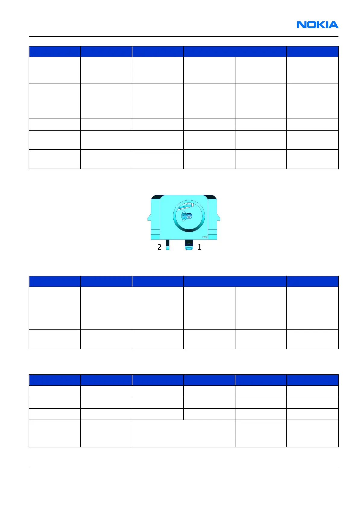
Charger connector and charging interface connections & electrical characteristics
Figure 109 Charger connector
Table 22 Charging interface connections
Pin Signal I/O Engine connection Notes
1 Vchar In N2300 VCharIn1, 2 Charging
voltage /
charger
detection,
Center pin
2 Charge GND Ground Charger
ground
Table 23 Charging IF electrical characteristics
Description Parameter Min Max Unit Notes
Vchar V Charge 0 9 V Center pin
Vchar I Charge 0.85 A Center pin
Charge GND 0.85 A
Threshold for
charging,
rising (N2300)
V
MSTR+
2.1 V Typical value
RM-180
System Module Nokia Customer Care
Issue 1 COMPANY CONFIDENTIAL Page 9 –37
Copyright © 2006 Nokia. All rights reserved.
 Loading...