Hardware description
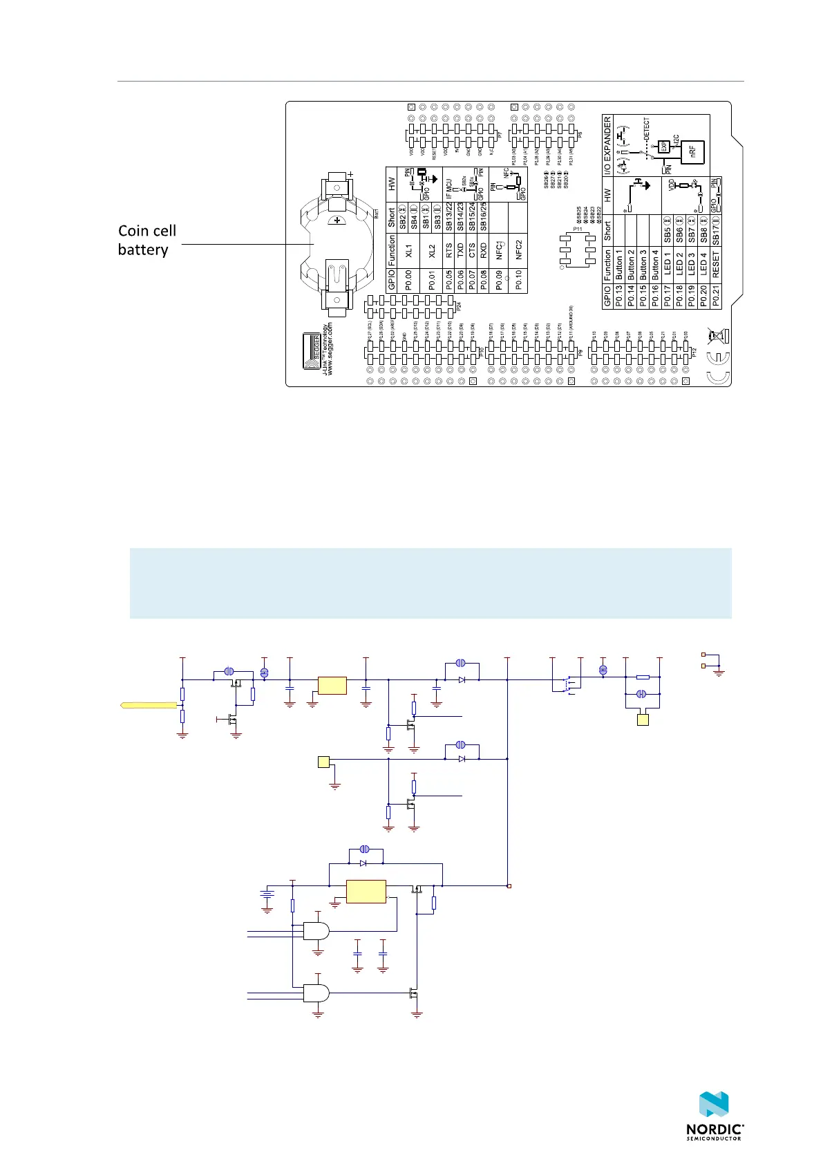
Figure 7: Power supply options (back)
The 5 V from the USB is regulated down to 3.3 V through an onboard voltage regulator. The battery and
external power supply are not regulated. The power from the regulator and external supply is routed
through diodes for reverse voltage protection (D1 and D7), where the circuit is supplied from the source
with the highest voltage. The power from the battery is routed through a load switch and a transistor.
These are controlled by the regulator voltage or external voltage, so if any of the two other sources are
present, the battery is disconnected from the circuit.
Note: When USB is not powered, the interface MCU is in dormant state and draws an additional
current of ~ 20 μA to maintain the reset button functionality. This affects current consumption, but
not the nRF52832 current measurements, as described in Measuring current on page 25.
Vin
GND
Vout
U3
AP7333-33SAG-7
VDD
R6
N.C.
SB9
VDD_nRFVBUS
SB10
SB11
2
P21
Pin List 1x2, Angled
1
2
P22
Pin List 1x2, Angled
VSUPPLY
R47
1M0
VSUPPLY
VEXT_DETECT
R46
1M0
VSUPPLY
R49
100k
Q4A
TSM250N02DCQ RFG
Q4B
TSM250N02DCQ RFG
R50
220k
R51
220k
D7
NSR0620P2T5G
D1
NSR0620P2T5G
Not mounted
D8
Figure 8: Power supply circuitry
4397_500
11