ML0021 August 15, 2018
v Copyright 2018 Bitronics, LLC
6.3.2 Physical .......................................................................................................................................... 84
6.4 Power Supply and Protective Ground (Earth) Connections .................................................................. 85
6.5 Overcurrent Protection .......................................................................................................................... 85
6.6 Supply/Mains Disconnect ...................................................................................................................... 85
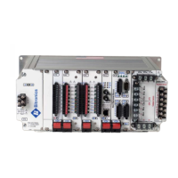
7.0 SIGNAL INPUT MODULE S10 - S12, S1C (M871), S13 - S17, S2C (M872) .......................................... 86
7.1 Introduction ............................................................................................................................................ 86
7.2 Features ................................................................................................................................................ 86
7.3 Specifications ........................................................................................................................................ 87
7.4 Current Input (CT) Connections ............................................................................................................ 93
7.5 Voltage Input (VT) Connections ............................................................................................................ 94
7.5.1 Overcurrent protection for Voltage input (VT) Connections ........................................................... 94
7.6 Current Measurements.......................................................................................................................... 95
7.6.1 Neutral Current (Residual Current) for WYE Connections ............................................................ 95
7.7 Voltage Measurements ......................................................................................................................... 95
7.8 Changing Transformer Ratios ............................................................................................................... 95
7.9 User (External Transformer) Gain and Phase Correction ..................................................................... 95
7.10 Calibration ........................................................................................................................................... 96
7.11 Installation and Calibration for the S1C Option ................................................................................... 96
8.0 ETHERNET MODULE P10, P11, P12 OR E1, E3 OPTION WITH H12 HOST ...................................... 108
8.1 Introduction .......................................................................................................................................... 108
8.2 Features .............................................................................................................................................. 109
8.3 Specifications (For P1x Modules Unless Otherwise Noted) ............................................................... 109
8.4 Environmental ..................................................................................................................................... 110
8.5 Physical ............................................................................................................................................... 110
8.6 Hot Swap (HS) Compatibility (P1x Modules) ...................................................................................... 110
8.7 Hardware Configuration ...................................................................................................................... 110
8.8 Cabling ................................................................................................................................................ 111
8.9 Connections ........................................................................................................................................ 111
8.10 Troubleshooting the Connection ....................................................................................................... 111
8.11 Indicators ........................................................................................................................................... 111
8.12 Software Configuration ...................................................................................................................... 112
8.13 Technical Details ............................................................................................................................... 112
8.13.1 Jumper Settings (P1x) ............................................................................................................... 114
8.13.2 Troubleshooting ......................................................................................................................... 115
8.13.3 PHYSTS Register Contents (P1x) ............................................................................................. 116
8.13.4 Statistics Gathered by Ethernet Driver ...................................................................................... 117
9.0 DIGITAL INPUT / OUTPUT MODULE P30A, P31, P33 ......................................................................... 118
9.1 Introduction .......................................................................................................................................... 118
9.2 Features .............................................................................................................................................. 118
9.3 Specifications ...................................................................................................................................... 119
9.4 Environmental ..................................................................................................................................... 120
9.5 Physical ............................................................................................................................................... 120
9.6 Hot Swap (HS) Compatibility ............................................................................................................... 120
9.7 Description ........................................................................................................................................... 120
9.7.1 P30A ............................................................................................................................................. 120
9.7.2 P31 ............................................................................................................................................... 121
9.7.3 P33 ............................................................................................................................................... 121
9.8 System Design Considerations ........................................................................................................... 121
9.8.1 Input / Output Impedance ............................................................................................................. 121
9.8.2 Input Assignments ....................................................................................................................... 121
9.9 Debounce Time Setting ....................................................................................................................... 122
9.10 Setting Digital I/O Module Jumpers ................................................................................................... 125
9.10.1 Disassembly of the P30A Module .............................................................................................. 125
9.10.2 Disassembly of the P31 Module ................................................................................................ 125
9.10.3 CompactPCI
TM
Interface Board (692) Jumper Settings ............................................................. 126
9.10.4 I/O Board (693) Jumper Settings ............................................................................................... 127
9.10.5 Health Status Digital Output Setting (Optional assignment of Digital Output 1 of Module 0) .... 129