NXP Semiconductors
KW45B41Z-EVKUM
KW45B41Z-EVK Board User Manual
Board feature Target MCU feature used Description
Power supply • The board can be powered up through:
– Coincell battery
– USB micro-B connector
– DC power jack
– CAN header
– LIN header
– Arduino socket power connector
– VBAT header (DNP)
• Following power configuration modes are supported:
– DC-DC Converter with Buck mode
– DC-DC Converter with Bypass mode
– PMIC mode
– Smart Power Switch mode
Clock The target MCU receives the following two clocks:
• A 32 MHz clock from a crystal for Arm core and radio.
Alternatively, the 32 MHz clock can be provided from a
TCXO (not populated on the board).
• A 32.768 kHz clock from another crystal as RTC and low-
power RF clock
Debug • Onboard MCU-Link debug probe with CMSIS-DAP and
SEGGER J-Link protocol options. It can connect to the
target MCU through a USB-to-UART, USB-to-SPI, or USB-
to-I2C bridge.
• 10-pin Arm JTAG/SWD connector for connecting an
external debug probe
Table 3. KW45B41Z-EVK features...continued
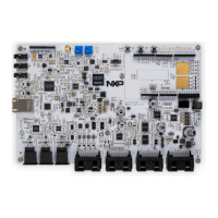
1.7 Board pictures
Figure 2 shows the top-side view of the KW45B41Z-EVK board, with connectors, push buttons, and LEDs
highlighted.
KW45B41Z-EVKUM All information provided in this document is subject to legal disclaimers. © 2023 NXP B.V. All rights reserved.
User manual Rev. 2 — 13 February 2023
7 / 50
 Loading...