NXP Semiconductors
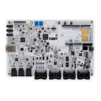
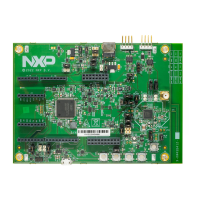
KW45B41Z-EVKUM
KW45B41Z-EVK Board User Manual
LPI2C module 8-bit I2C address Device Description
KW45B41Z (U1) Target MCU. It acts as I2C master for all
I2C connections on the board except for I2C
connection with MCU-Link.
LPC55S69JBD100 (U13) MCU-Link. A USB-to-I2C bridge is supported
between MCU-Link and the target MCU using
an I2C repeater / voltage translator U27. This
I2C connection can be used for debugging the
target MCU (I2C slave) from MCU-Link (I2C
master). Jumper JP30 can be used to enable/
disable the USB-to-I2C bridge.
• Read address: 0xC3
• Write address: 0xC2
PCA9420UK (U2) Power management integrated circuit (PMIC)
• Read addresses:
0x33, 0x31
• Write addresses:
0x32, 0x30
FXLS8964AF (U12) Accelerometer
I2C address is defined
by the plugged-in click
board
mikroBUS socket connector
J13
Allows an I2C connection between the target
MCU and plugged-in click board
LPI2C1
I2C address is defined
by the plugged-in
Arduino board
Arduino socket DH connector
J2
Allows an I2C connection between the target
MCU and plugged-in Arduino board
Table 15. KW45B41Z-EVK LPI2C bus device map
2.7 RF interface
The target MCU integrates a high-performance radio transceiver, which includes a Bluetooth Low Energy
(LE) version 5.3 radio. The radio transceiver operates in the 2.4 GHz frequency band, supporting Gaussian
frequency shift keying (GFSK) modulations for Bluetooth LE 5.3.
The KW45B41Z-EVK board provides a small-footprint, low-cost RF interface for users to begin application
development. Table 16 describes the features of the KW45B41Z-EVK RF interface.
Feature Description
Input/output port Single-ended RF input/output port (one of the following ports is available at a time):
• PCB-integrated inverted-F antenna ANT1 (enabled by default)
• SMA connector J7 (SLE-100010072-F01)
External component
requirement
Very few external components are required
Output power Programmable output power from -30 dBm to +10 dBm at the SMA connector in DC-DC
Bypass, DC-DC Buck, or Smart Power Switch mode
Typical receiver sensitivity • -103 dBm for GFSK applications (250 kbit/s GFSK-BT = 0.5, h = 0.5)
• -106 dBm for Bluetooth LE LR 125 kbit/s applications
• -102 dBm for Bluetooth LE LR 500 kbit/s applications
• -97.5 dBm for Bluetooth LE 1 Mbit/s applications
• -95 dBm for Bluetooth LE 2 Mbit/s applications
Table 16. RF interface features
Figure 21 shows the KW45B41Z-EVK RF diagram.
KW45B41Z-EVKUM All information provided in this document is subject to legal disclaimers. © 2023 NXP B.V. All rights reserved.
User manual Rev. 2 — 13 February 2023
35 / 50
 Loading...