287
Auxiliary Area and CIO Area Allocations (Modbus-RTU Slave Mode) Section 9-3
Response
Writing 1 (ON) to
CIO 0002.02
Note The shaded number indicate the ON/OFF status of the bit that is written.
Write Single Register
Function Writes a word in the DM or EM Area of I/O memory.
Command
Note The address depends on the area that is allocated.
Response
Writing 3AC5 Hex to
D2000
Length Data
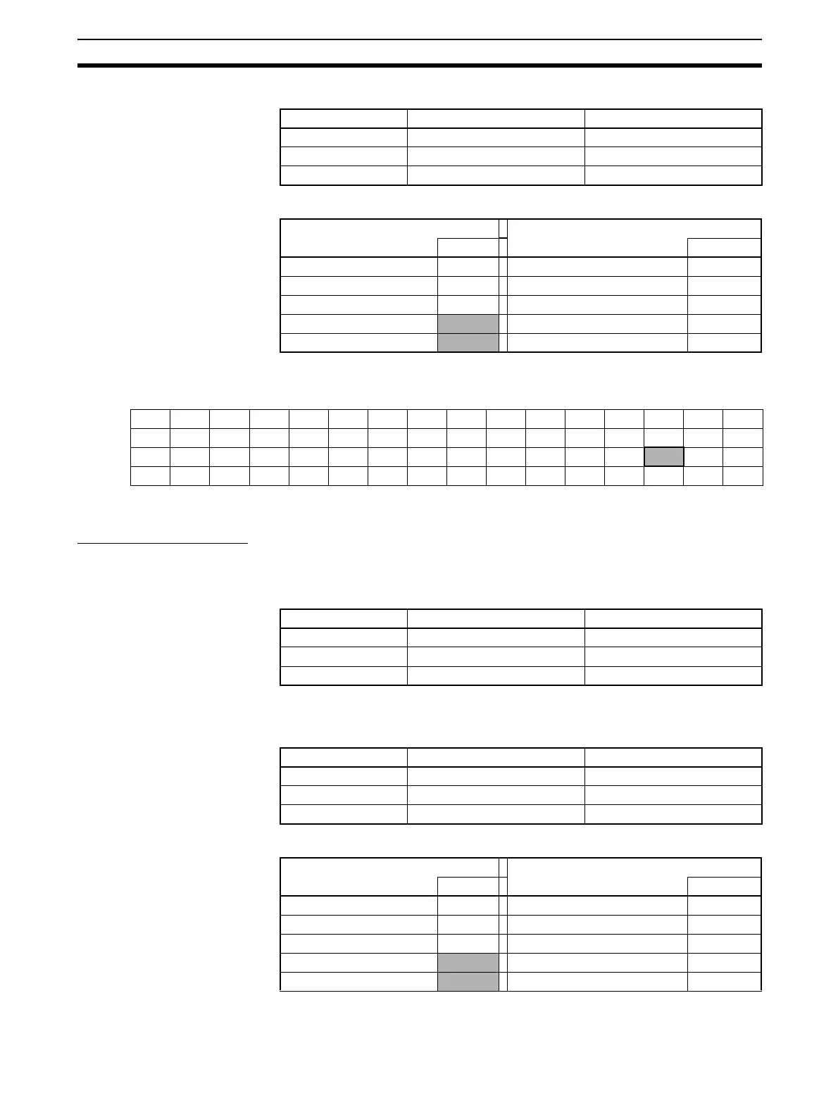
Function Code 1 byte 05 hex
Output Address 2 bytes 0 to FFFF hex
Output Value 2 bytes 0000 hex (OFF) or FF00 (ON)
Request Response
Data Data
Function Code 05 hex Function Code 05 hex
Output Address (H) 00 hex Output Address (H) 00 hex
Output Address (L) 22 hex Output Address (L) 22 hex
Output Value (H)
FF hex Output Value (H) FF hex
Output Value (L)
00 hex Output Value (L) 00 hex
1514131211109876543210
CIO 01514131211109 8 7 6 5 4 3 2 1 0
CIO 131302928272625242322212019181716
CIO 247464544434241403938373635
34 33 32
CIO 363626160595857565554535251504948
Length Data
Function Code 1 byte 06 hex
Register Address 2 bytes 0 to 7FFF hex (See note.)
Register Value 2 bytes 0 to FFFF hex
Length Data
Function Code 1 byte 06 hex
Register Address 2 bytes 0 to 7FFF hex
Register Value 2 bytes 0 to FFFF hex
Request Response
Data Data
Function Code 06 hex Function Code 06 hex
Register Address (H) 07 hex Register Address (H) 07 hex
Register Address (L) D0 hex Register Address (L) D0 hex
Register Value (H)
3A hex Register Value (H) 3A hex
Register Value (L)
C5 hex Register Value (L) C5 hex
 Loading...