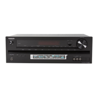
TX-SR606
IC BLOCK DIAGRAMS AND TERMINAL DESCRIPTIONS-26
Q8001 : FLI30502 (LCD TV Controller with Worldwide Standard Sound Processor
and HDMI Receiver)-8/12
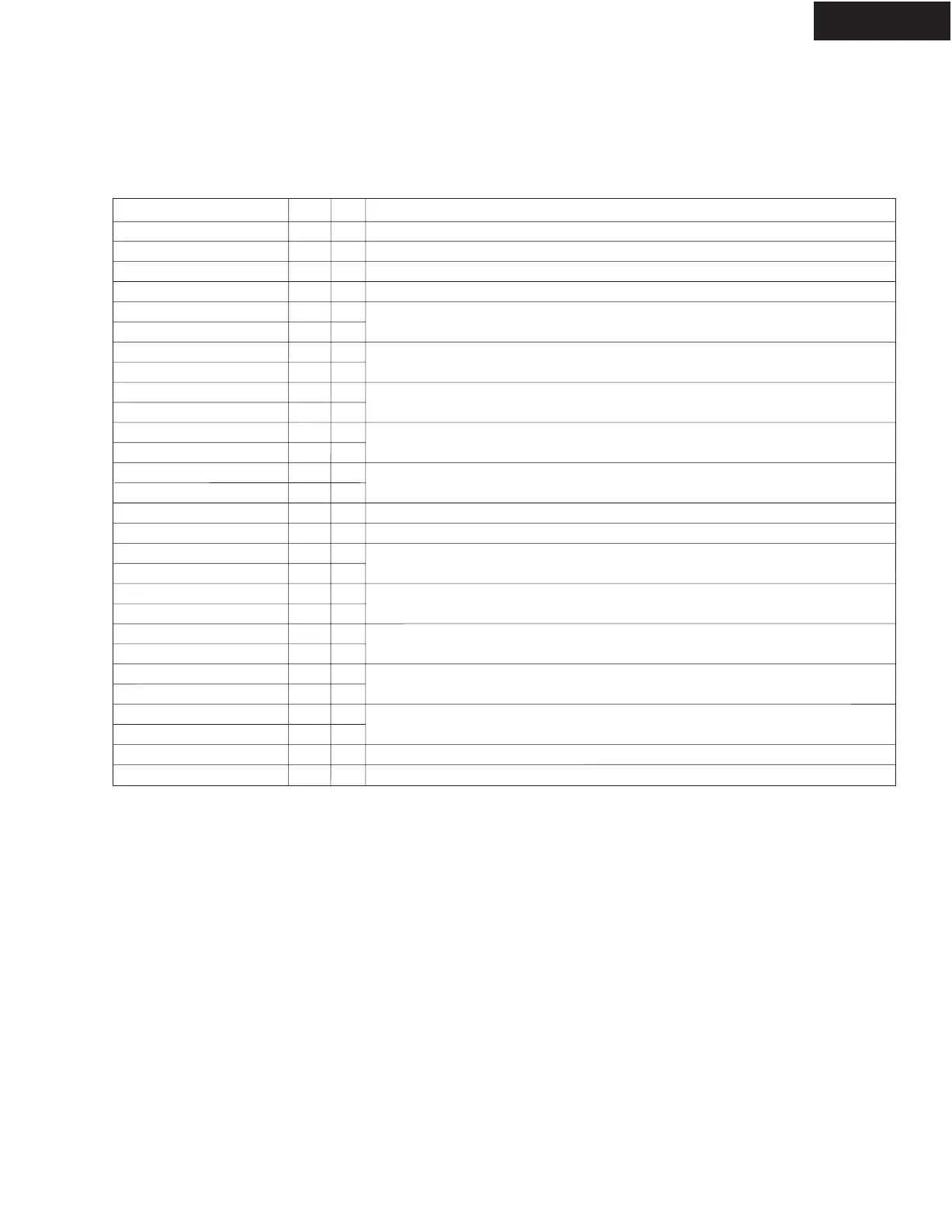
TERMINAL DESCRIPTION
LVDS Display interface
I/O
O
O
DP
G
O
O
O
O
O
O
O
O
O
O
G
DP
O
O
O
O
O
O
O
O
O
O
G
DP
Description
Panel Bias Control (backlight enable, tri-state output, 5 V tolerant).
Panel Power Control (tri-state output, 5 V tolerant).
Digital Power for LVDS Block. Connect to digital 3.3V supply.
Ground for LVDS outputs.
These form the Differential Data Output for Channel 3 (Even).
These form the Differential Clock Output Even Channel.
These form the Differential Data Output for Channel 2 (Even).
These form the Differential Data Output for Channel 1 (Even).
These form the Differential Data Output for Channel 0 (Even).
Ground for LVDS outputs.
Digital Power for LVDS outputs. Connect to digital 3.3 V supply.
These form the Differential Data Output for Channel 3 (Odd).
These form the Differential Clock Output Odd Channel.
These form the Differential Data Output for Channel 2 (Odd).
These form the Differential Data Output for Channel 1 (Odd).
These form the Differential Data Output for Channel 0 (Odd).
Ground for LVDS outputs.
Digital Power for LVDS outputs. Connect to digital 3.3 V supply.
Pin Name
PBIAS
PPWR
AVDD_LV_33
AVSS_LV
CH3P_LV_E
CH3N_LV_E
CLKP_LV_E
CLKN_LV_E
CH2P_LV_E
CH2N_LV_E
CH1P_LV_E
CH1N_LV_E
CH0P_LV_E
CH0N_LV_E
VSS_OUT_LV
VDD_OUT_LV_33
CH3P_LV_O
CH3N_LV_O
CLKP_LV_O
CLKN_LV_O
CH2P_LV_O
CH2N_LV_O
CH1P_LV_O
CH1N_LV_O
CH0P_LV_O
CH0N_LV_O
AVSS_OUT_LV
AVDD_OUT_LV_33
Pin #
71
72
74
73
75
76
77
78
79
80
81
82
83
84
85
86
87
88
89
90
91
92
93
94
95
96
97
98
 Loading...