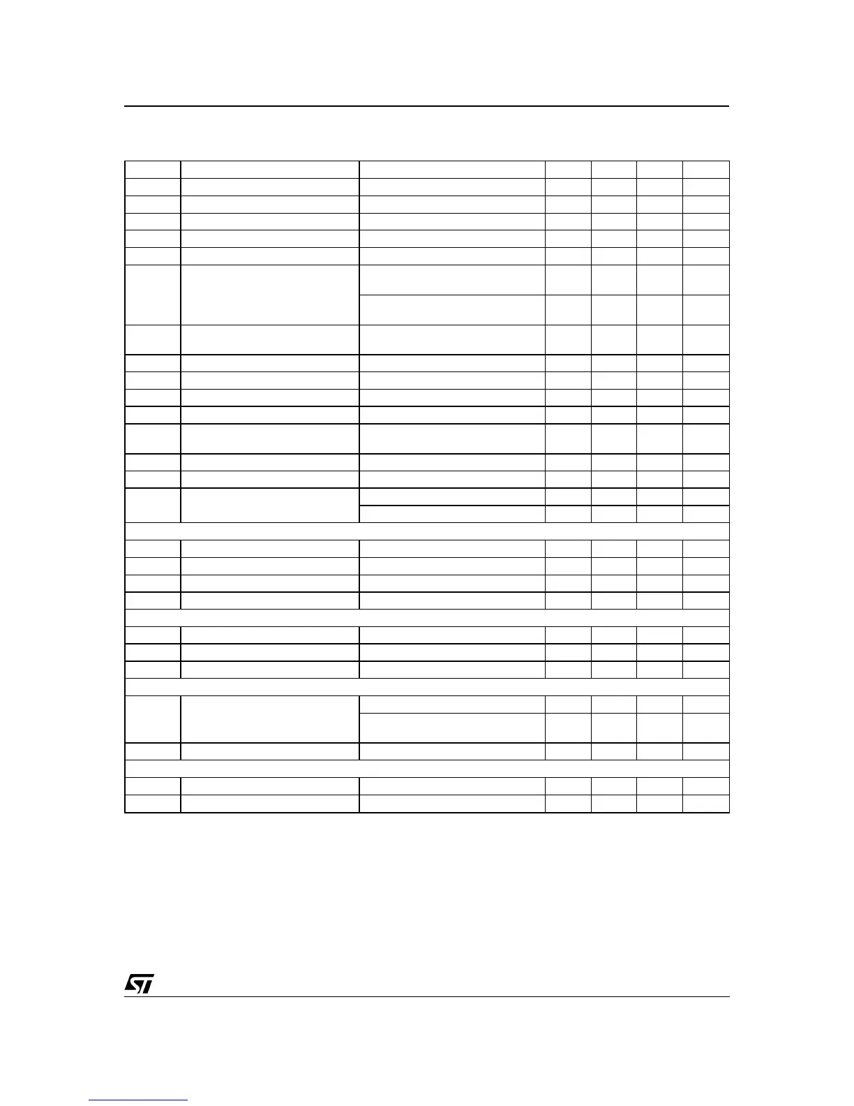
ELECTRICAL CHARACTERISTICS (Refer to the Test Circuit V
S
= ±40V, R
L
= 8Ω, R
g
= 50 Ω;
T
amb
= 25°C, f = 1 kHz; unless otherwise specified).
Symbol Parameter Test Condition Min. Typ. Max. Unit
V
S
Supply Range
±
12
±
50 V
I
q
Quiescent Current 50 100 mA
I
b
Input Bias Current 0.3 1
µ
A
V
OS
Input Offset Voltage -10 10 mV
I
OS
Input Offset Current 0.2
µ
A
P
O
RMS Continuous Output Power d = 1%:
R
L
= 4
Ω;
V
S
=
±
29V,
75 80
80
W
d = 10%
R
L
= 4
Ω
; V
S
=
±
29V
90 100
100
W
d Total Harmonic Distortion (**) P
O
= 5W; f = 1kHz
P
O
= 0.1 to 50W; f = 20Hz to 15kHz
0.005
0.1
%
%
I
SC
Current Limiter Threshold V
S
≤
±
40V 6.5 A
SR Slew Rate 5 10 V/
µ
s
G
V
Open Loop Voltage Gain 80 dB
G
V
Closed Loop Voltage Gain (1) 29 30 31 dB
e
N
Total Input Noise A = curve
f = 20Hz to 20kHz
1
310
µ
V
µ
V
R
i
Input Resistance 100 k
Ω
SVR Supply Voltage Rejection f = 100Hz; V
ripple
= 0.5Vrms 75 dB
T
S
Thermal Protection DEVICE MUTED 150
°
C
DEVICE SHUT DOWN 160
°
C
STAND-BY FUNCTION
(Ref: to pin 1)
V
ST on
Stand-by on Threshold 1.5 V
V
ST off
Stand-by off Threshold 3.5 V
ATT
st-by
Stand-by Attenuation 70 90 dB
I
q st-by
Quiescent Current @ Stand-by 0.5 1 mA
MUTE FUNCTION
(Ref: to pin 1)
V
Mon
Mute on Threshold 1.5 V
V
Moff
Mute off Threshold 3.5 V
ATT
mute
Mute AttenuatIon 60 80 dB
CLIP DETECTOR
Duty Duty Cycle ( pin 5) THD = 1% ; RL = 10K
Ω
to 5V 10 %
THD = 10% ;
RL = 10K
Ω
to 5V
30 40 50 %
I
CLEAK
PO = 50W 3
µ
A
SLAVE FUNCTION pin 4
(Ref: to pin 8 -V
S
)
V
Slave
SlaveThreshold 1V
V
Master
Master Threshold 3 V
Note (1):
G
Vmin
≥
26dB
Note:
Pin 11 only for modular connection. Max external load 1M
Ω
/10 pF, only for test purpose
Note (**):
Tested with optimized Application Board (see fig. 2)
TDA7293
3/15
 Loading...