INTRODUCTION
In consumer electronics, an increasing demand
has arisen for very high power monolithic audio
amplifiers able to match, with a low cost, the per-
formance obtained from the best discrete de-
signs.
The task of realizing this linear integrated circuit
in conventional bipolar technology is made ex-
tremely difficult by the occurence of 2nd break-
down phoenomenon. It limits the safe operating
area (SOA) of the power devices, and, as a con-
sequence, the maximum attainable output power,
especially in presence of highly reactive loads.
Moreover, full exploitation of the SOA translates
into a substantial increase in circuit and layout
complexity due to the need of sophisticated pro-
tection circuits.
To overcome these substantial drawbacks, the
use of power MOS devices, which are immune
from secondary breakdown is highly desirable.
The device described has therefore been devel-
oped in a mixed bipolar-MOS high voltage tech-
nology called BCDII 100/120.
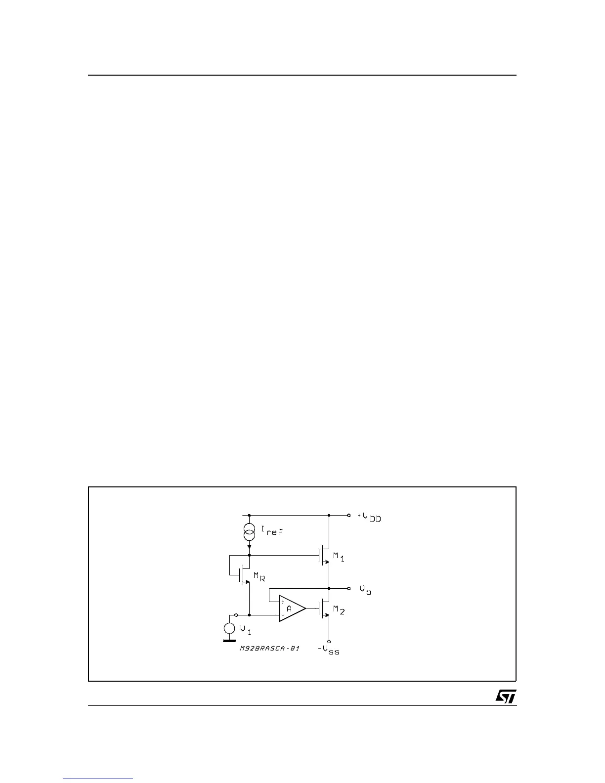
1) Output Stage
The main design task in developping a power op-
erational amplifier, independently of the technol-
ogy used, is that of realization of the output stage.
The solution shown as a principle shematic by
Fig3 represents the DMOS unity - gain output
buffer of the TDA7293.
This large-signal, high-power buffer must be ca-
pable of handling extremely high current and volt-
age levels while maintaining acceptably low har-
monic distortion and good behaviour over
frequency response; moreover, an accurate con-
trol of quiescent current is required.
A local linearizing feedback, provided by differen-
tial amplifier A, is used to fullfil the above require-
ments, allowing a simple and effective quiescent
current setting.
Proper biasing of the power output transistors
alone is however not enough to guarantee the ab-
sence of crossover distortion.
While a linearization of the DC transfer charac-
teristic of the stage is obtained, the dynamic be-
haviour of the system must be taken into account.
A significant aid in keeping the distortion contrib-
uted by the final stage as low as possible is pro-
vided by the compensation scheme, which ex-
ploits the direct connection of the Miller capacitor
at the amplifier’s output to introduce a local AC
feedback path enclosing the output stage itself.
2) Protections
In designing a power IC, particular attention must
be reserved to the circuits devoted to protection
of the device from short circuit or overload condi-
tions.
Due to the absence of the 2nd breakdown phe-
nomenon, the SOA of the power DMOS transis-
tors is delimited only by a maximum dissipation
curve dependent on the duration of the applied
stimulus.
In order to fully exploit the capabilities of the
power transistors, the protection scheme imple-
mented in this device combines a conventional
SOA protection circuit with a novel local tempera-
ture sensing technique which " dynamically" con-
trols the maximum dissipation.
Figure 3: Principle Schematic of a DMOS unity-gain buffer.
TDA7293
6/15
 Loading...