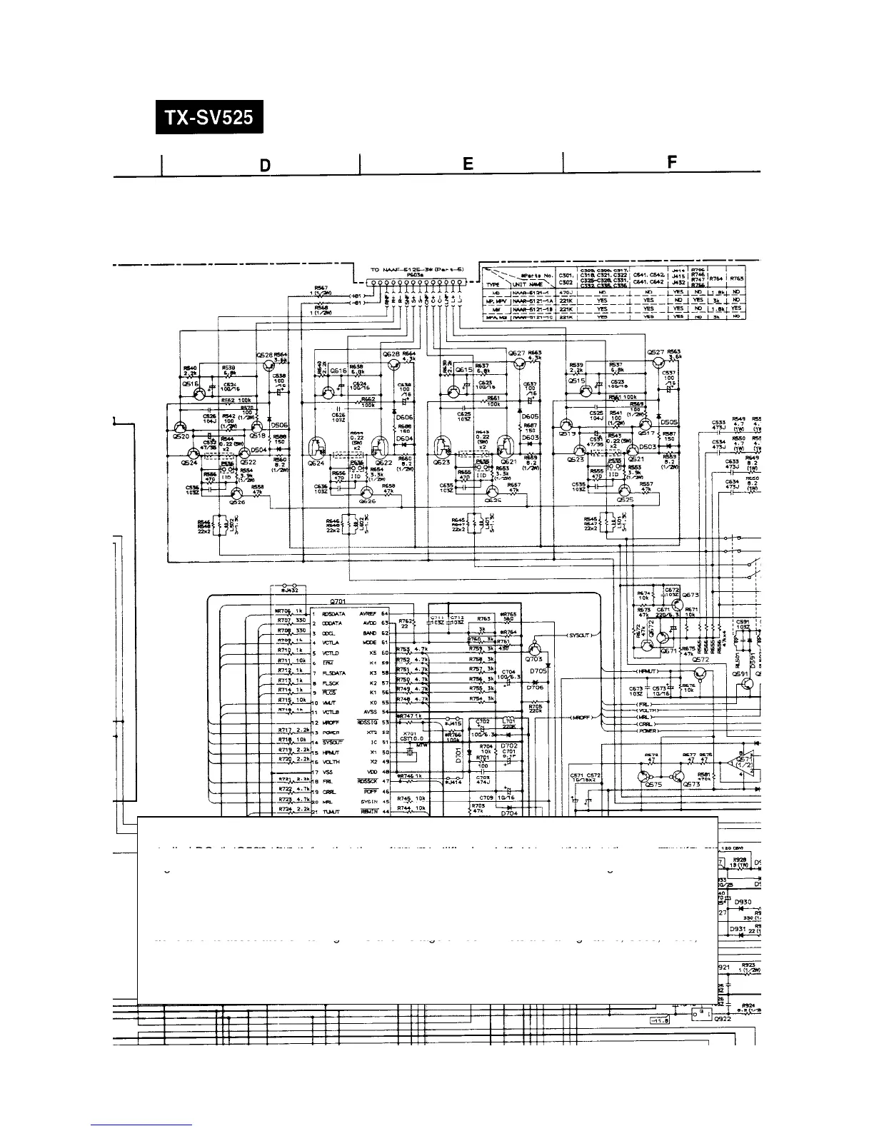
It should be clear that the base of Q520 should not be more than -1 2vdc and Q518 +1 3vdc Q516 is
.
.
.
the bias and its turn on is the potential difference of RC components R540 and R538. Q518 also gets its
t ll d DC i Q526 A i th t th lt lifi i ki tl th th t f
con
ro
e
v
a
.
ssum
ng
a
e vo
age amp
er
s wor
ng correc
y,
en
e amoun
o
volta
e delivered at the base of Q520 and Q518 should be within the tolerance to be
overned
(controlled) by Q516.
In general practice two possibilities exist in this case
.
1. The base drive voltage coming from Voltage amplifier stage arriving at Q518 and Q520 is to high to
be controlled by Q516 and its associated components.
2. Q516 and its associated switching
+
-
Nets are failing. Q526, C538, D506,
D504, R562, are all part of the Q516 operators service as reference control to the bias.
Is the problem 1 or 2 or both?
 Loading...