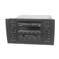
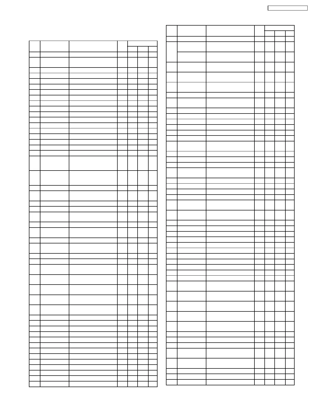
11.1. Main Block
IC601 : C2CBJG000589
Pin
No.
Port Description (I/O) (V)
FM AM CD
1 PANEL OPEN PANEL OPEN detection I 0 5.2 5.2
2 PANEL
CLOSE
PANEL CLOSE detection I 0 0 5.2
3 NC No Connection - - - -
4 BATT BATT detection I 4.8 5 5
5 ACC ACC detection I 4.8 5 5
6 SDA Electronic VOL data I/O 4.9 4.9 4.9
7 SCLK Electronic VOL clock O 4.9 4.9 4.9
8 NC No Connection - - - -
9 Vss Power supply GND I 0 0 0
10 ST FM ST detection I 5.1 5.2 5.2
11 PLL DI(MO) PLL data output O 0.6 0 0
12 PLL DO(MI) PLL data input I 5.2 5.2 5.2
13 PLL CLK PLL clock output O 4.9 4.9 4.9
14 PLL CE PLL chip enable output O 0 0 0
15 CD RST CD deck reset output O 4.9 4.9 4.9
16 SUB SI SUB u-com Data trans SO 0.6 0.6 0.8
17 NC No Connection - - - -
18 SUB SO SUB u-com data recept SI 4.4 4.4 4.4
19 CH DATA Changer; data
transmission from XM;
FLASH W SO
SI 1.6 1.6 1.6
20 CH CLK Clock transmission from
the changer; FLASH W
CLK
SCK 4.9 4.9 4.9
21 Vdd Power supply I 4.9 4.9 4.9
22 XM SI DATA transmission to
XM; FLASH W SI
S0 0 0 0
23 CD SI CD DATA transmission S0
24 CD SCK CD Clock transmission SCK 0 0.4 0
25 CONDENSOR Capacitor for power
supply
- 3.3 3.3 3.3
26 CDC SO CD DATA transmission SI 0 0 0
27 CDC STB Changer stororb signal
input
INT 0 0 0
28 CD IN DISC in detect I 4.9 4.9 0.4
29 DECK V
CONT
DECK power supply
control output
O 4.9 4.9 4.9
30 CD STB CD frame sink O 3.7 3.7 3.7
31 NC No Connection - - - -
32 Avdd Power supply of D/A
converter
I 5.1 5.1 5.1
33 AVREF Reference voltage for
D/A converter
I 5.1 5.1 5.1
34 AVGND Reference GND for D/A
converter
I 0 0 0
35 AVSS Grand for A/D and D/A
converter
I 0 0 0
36 SD FM/AM signal meter
signal input
A/D 0.2 0 0.3
37 INIT A Initializ A A/D 0 0 0
38 INIT B Initializ B A/D 0 0 0
39 AIN SPE.ANA A.IN A/D 0 0 0
40 Vss GND I 0 0 0
41 CD MUTE CD deck mute detection I 0 0 5.1
42 NC No Connection - - - -
43 NC No Connection - - - -
44 NC No Connection - - - -
45 CD SW1 CD disc in detection I - - -
46 CD SW2 CD disc in detection I - - -
47 MOD0 Operating mode input 0 I 5.1 5.1 5.1
48 MOD1 Operating mode input 1 I 5.1 5.1 5.1
49 MOD2 Operating mode input 2 I 0 0 0
Pin
No.
Port Description (I/O) (V)
FM AM CD
50 H STANDBY External standby input I 5 5 5
51 DC DC CNT DC/DC control for 60W
(CQ-C8401W)
O 0 0 0
NC No Connection
(CQ-C7401W)
- - - -
52 FP MOTOR1 Front open/close control
1
O 4.9 5 4.9
53 FP MOTOR2 Front open/close control
2
O 4.9 5 4.9
54 V CNT1 Panel driving voltage
control 1
O 0 0 5
55 V CNT2(NC) No Connection - - - -
56 SA CLK Control for Speana
acquisition
O 5 5 4.9
57 EXT MUTE TEL/NAVI MUTE input I 5.3 5.2 5.2
58 AMP CONT External AMP control O 4.9 5 4.9
59 BZ-OUT Buzzer output PPG 0 0 0
60 ANT CONT Motor antenna control O 4.9 5 0
61 DIM1 Dimmer control output 1 O 0 0 0
62 DIM2 Dimmer control output 2 O 0 0 0
63 CDC REM
OUT
Remote control code
output to Changer
O 5 5 5
64 CDC SENS CDC 1/2 detection I 5.1 5.1 5.1
65 CDC 1/2 CDC 1/2 change output O 0 0 0
66 NC No Connection - - - -
67 MWUP MAIN.WAKE.UP.REQ
input
I 5 4.9 5
68 NC No Connection - - - -
69 NC No Connection - - - -
70 NC No Connection - - - -
71 NC No Connection - - - -
72 MAIN CONT MAIN power supply
control output
O 4.9 4.9 4.9
73 INV CONT INV power supply control
output
O 5 5 5
74 AF MUTE Tr-MUTE control O/I 5 5 5
75 RESET Reset input I 5 5 5
76 NC No Connection - - - -
77 NC No Connection - - - -
78 NC GND I 0 0 0
79 Vss GND I 0 0 0
80 X1 Crystal oscillator input I 2 2 2
81 X2 Crystal oscillator output O 2.5 2.5 2.5
82 Vdd Power supply I 5 5 5
83 P00 Pldaun port for writing I 0 0 0
84 P01 Pull-up port for writing I 5.1 5 5.1
85 OFFSET DET PWR-IC OFFSET
detection
I 0 0 0
86 STBY PWR-IC STBY control
output
O 5 5 5
87 AMP MUTE PWR-IC MUTE control
output
O 0 0 0
88 ILL SENS External dimmer control
input
I 5 5 5
89 SUBM CNT 3.3V control for SUB
microcomputer
O 5 5 5
90 NC No Connection - - - -
91 NC No Connection - - - -
92 NC No Connection - - - -
93 SUB W U
REQ
SUB.WAKE.UP.REQ O 4.9 5 4.9
94 DISPM CNT Power supply control
output of display 5V
O/I 0 0 0
95 EJE ILL(NC) No Connection - - - -
96 NC No Connection - - - -
97 NC No Connection - - - -
11 TERMINALS DESCRIPTION
13
CQ-C8401W / CQ-C7401W
 Loading...