Averaging for Voltage Ranges and Current RangesFP0 A/D Converter Unit
5 − 3
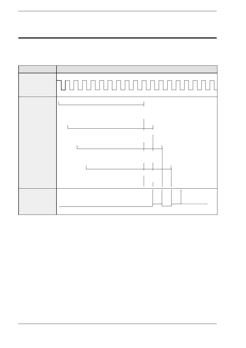
5.1 Averaging Function
5.1 Averaging Function
When the averaging function is set to on, the internal processing of the A/D conversion
unit is as shown in the diagram below (in this example there are two input channels, and
the input range setting switch Nos. 3 and 4 are off).
Operation item Time chart
Analog input
value for ch0
(Reading time)
ch1
1800
1ms
1ms
1ms
ch0
1780 1820 1790 1800 1850 1900 1830 1870 1910 1780 1810 1950
ch1
ch0
ch1
ch0
ch1
ch0
ch1
ch0
ch1
ch0
ch1
ch0
ch1
ch0
ch1
ch0
ch1
ch0
ch1
ch0
ch1
ch0
ch1
ch0
ch1
ch0
ch1
ch0
ch1
ch0
ch1
ch0
ch1
ch0
Internal
processing for
A/D conversion
unit ch0
1800 1780 1820 1790 1800 1850 1900 1830 1870
(1800+1820+1790+1800+1850+1900+1830+
1870)
÷8=1832.50
min
1780 1820 1790 1800 1850 1900 1830 1870
(1820+1790+1800+1850+1900+1830+
1870+1780)
÷8=1830.00
min
1820 1790 1800 1850 1900 1830 1870
(1820+1790+1800+1850+1900+
1830+1870+1810)÷8=1833.75
1790 1800 1850 1900 1830 1870
max
1810 1950
(1790+1800+1850+1900+
1830+1870+1910+1810)
÷
=1845
1910
1910
max
1910
max min
1810
max
8
veraging of results
rom 8 times, with
max/min values deleted.
deleted deleted
deleted
deleted
deleted
deleted
deleted
1780
1910
deleted
min
1780
1780
Digital output
value for ch0
K1832
K1830
K1833 K1845
The largest and smallest values from the most recent 10 data values are deleted, and
the remaining eight values are averaged and output on WX2 and WX3. The values
output at this time always use the most recent averaged value (decimals are discarded).