Do you have a question about the Panasonic KX-FLM551 and is the answer not in the manual?
Essential safety guidelines for servicing, including power disconnection, proper parts usage, and cord checks.
Procedure to test insulation resistance using an ohmmeter to prevent shock hazards after servicing.
Precautions for service technicians to prevent static electricity damage to ICs and LSIs during repairs.
Warning about battery replacement risks, emphasizing correct type and proper disposal procedures.
Safety steps before closing the cabinet, ensuring earth lead is fixed and AC connector is properly connected.
Precautions concerning moving parts of the unit and live electrical sections during service.
General service precautions to prevent static electricity damage and ensure safety.
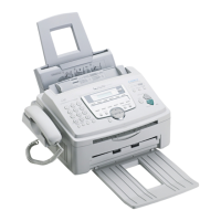
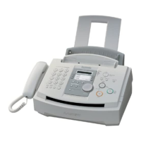
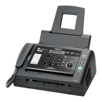
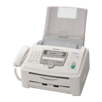
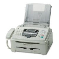
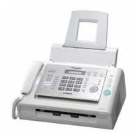
Overview of unit features, including help function, display options, and operational capabilities.
Technical specifications covering applicable lines, caller ID, memory, laser properties, and OS compatibility.
List of optional accessories available for the unit, such as toner cartridges and drum units.
Diagrams and descriptions of the unit's controls, including rear view and control panel layout.
Instructions for connecting the handset cord, telephone line cord, and power cord for initial setup.
Guidelines for unit installation, covering space requirements, environment, and power cord length.
General troubleshooting steps and precautions to identify and resolve unit problems effectively.
List of display messages indicating recoverable errors and their causes and remedies.
Detailed troubleshooting procedures, including outlines, starting steps, and item tables for problem diagnosis.
Information on programming functions, user mode, service mode, and accessing system setup lists.
List of test functions for performing simple checks on unit functions to identify malfunction causes.
Instructions for connecting the fax machine to a computer for various functions like printing and scanning.
Step-by-step guide for installing the necessary software on a computer.
Troubleshooting common issues related to the PC software, including scanning and file compatibility.
Detailed procedure for removing the bottom plate, drum unit, and paper tray assembly.
Step-by-step instructions for safely removing the operation panel block.
Procedure for removing the operation board from the unit.
Instructions for removing the transfer roller and image sensor components.
Procedure for removing the separation rubber and document feed roller.
Instructions for removing analog board, varistor board, laser scanning unit, and speaker.
Procedure for removing the AC inlet and low voltage power supply board.
Instructions for removing the digital board and motor drive board.
Step-by-step guide for removing the back cover section of the unit.
Procedure for removing the fuser unit and handset cradle.
Instructions for removing the main frame and fan.
Procedure for removing the high voltage power supply board.
Instructions for removing the heat roller and exit roller.
Procedure for removing the pressure roller assembly.
Instructions for removing the motor block assembly.
Diagrams showing the correct installation positions for lead wires during reassembly.
Preparation steps for replacing Flat Package ICs, listing necessary tools like solder and soldering iron.
Procedure for removing Flat Package ICs, including solder application and pin cutting techniques.
Steps for installing a new Flat Package IC, covering temporary fixing and flux application.
Procedure for modifying bridge connections, involving resoldering and removing excess solder.
Diagram illustrating the printing process chart and associated process bias values.
Explanation of the charging stage, detailing surface potential control of the sensitive drum.
Description of the exposing stage, where laser irradiation creates an invisible image on the drum.
Diagrams showing the locations of components within the Laser Scanning Unit.
Explanation of developing and transcription stages, covering toner transfer to drum and paper.
Description of the cleaning stage for removing residual toner from the OPC drum.
Explanation of the fixing stage, where toner is permanently attached to paper using heat and pressure.
Timing chart illustrating the sequence of operations during printing.
Explanation of the image reading part, including the automatic document feeder and CIS.
Overview of the document transmission process.
Description of the printing process, detailing gear operations and motor pinion rotation.
Explanation of the paper pickup mechanism, including gears, solenoid, and plate lift.
Explanation of initialization types (short and long) and their functions.
Timing chart illustrating the sequence of operations during short initialization.
Timing chart illustrating the sequence of operations during long initialization.
Diagrams illustrating the connection of various components and boards within the unit.
Overview of the general block diagram, outlining the function of each IC on the digital board.
Explanation of the digital block diagram, detailing CPU, RTC, DECODER, ROM/RAM, and ASIC functions.
Diagram illustrating the memory map, showing assignments for Flash ROM, SRAM, and other memory types.
Explanation of the SRAM and RTC backup circuit, powered by a lithium battery.
Function of the modem section, handling FAX transmission and reception via CODEC and ASIC.
Details on the analog section, including signal routing and level adjustments via the analog gate array.
General information about the telephone line interface, including EXT. TEL relay and TAM interface circuit.
Explanation of the TAM interface circuit, switching between FAX and external TAM operation.
Explanation of the CIS control section, including its circuit and how it processes scanned documents.
Explanation of the stepping motor drive section, detailing its functions and motor operation.
Information about the fan motor section, used for radiating heat and controlling rotation speed.
Explanation of the solenoid drive circuit controlling the pick-up clutch.
Details on the LSU section, including its optical components and signal path.
Overview of sensors and switches, including their locations, names, and associated error messages.
Information about the operation board, including LCD, keys, LEDs, and sensors.
Explanation of the LCD section, its interface circuitry, and density control.
Specifications and circuit diagrams for the High Voltage Power Supply (HVPS) section.
Explanation of the heat lamp control circuit, including thermistor, thermal fuse, and thermostat functions.
Schematic diagram for the digital board (PCB1), illustrating component layout and connections.
Schematic diagram for the analog board (PCB2), showing circuit operations and connections.
Schematic diagram for the operation board (PCB3), detailing key matrix and sensor connections.
Schematic diagram for the high voltage power supply board (PCB4), showing circuit operations.
Schematic diagram for the low voltage power supply board (PCB5).
General section showing the location of cabinet, mechanical, and electrical parts.
Diagrams showing the layout of the operation panel block components.
Diagram illustrating the layout of cabinet and PCB components.
Exploded view and part identification for the pick-up block assembly.
Exploded view and part identification for the cabinet block assembly.
Exploded view and part identification for the fuser block assembly.
Exploded view and part identification for the main frame block assembly.
Exploded view and part identification for the motor block assembly.
Illustrations showing the actual size of screws and washers used in the unit.
List of accessories and packing materials included with the unit.
Comprehensive list of replacement parts, including notes on markings, safety, and specifications.
List of replacement parts for the cabinet and electrical components.
List of replacement parts for the operation panel block.
List of replacement parts for cabinet and PCB blocks.
List of replacement parts for the pick-up block.
List of replacement parts for the cabinet block.
List of replacement parts for the fuser block.
List of replacement parts for the main frame block.
List of replacement parts for the motor block.
List of replacement parts for the digital board, including ICs, transistors, and diodes.
List of replacement parts for the analog board, including ICs, transistors, and diodes.
List of fixtures and tools required for servicing and maintenance tasks.
List of replacement parts for the low voltage power supply board.
List of replacement parts for the motor drive board.
List of replacement parts for the sensor board.
List of replacement parts for the varistor board.
Notes regarding schematic diagram usage, including voltage measurements and modifications.
Schematic diagram for the digital board (PCB1), illustrating component layout and connections.
Schematic diagrams for various boards: Analog, Operation, High Voltage, Low Voltage, Motor Drive, Sensor, and Varistor.
Schematic diagram for the analog board (PCB2), detailing circuit operations.
Schematic diagram for the operation board (PCB3), showing key matrix and sensor connections.
Schematic diagram for the high voltage power supply board (PCB4).
Schematic diagram for the low voltage power supply board (PCB5).
Schematic diagram for the motor drive board (PCB6).
Schematic diagram for the sensor board (PCB7).
Schematic diagram for the varistor board (PCB8).
Layouts for printed circuit boards, including component and bottom views.
Component and bottom views of the Digital Board (PCB1).
Component and bottom views of the Analog Board (PCB2).
Component and bottom views of the Operation Board (PCB3).
Component and bottom views of the High Voltage Power Supply Board (PCB4).
Component and bottom views of the Low Voltage Power Supply Board (PCB5).
Component and bottom views of the Motor Drive Board (PCB6).
Component and bottom views of the Sensor Board (PCB7).
Component and bottom views of the Varistor Board (PCB8).
| Printing Technology | Laser |
|---|---|
| Resolution | 600 x 600 dpi |
| Paper Capacity | 250 sheets |
| Modem Speed | 33.6 Kbps |
| ADF Capacity | 20 sheets |
| Memory Transmission | Yes |
| Copier Function | Yes |
| Caller ID | Yes |
| Connectivity | USB |
| Paper Handling | Automatic Document Feeder |
| Fax Features | Auto Redial |
| Type | Plain Paper Fax |