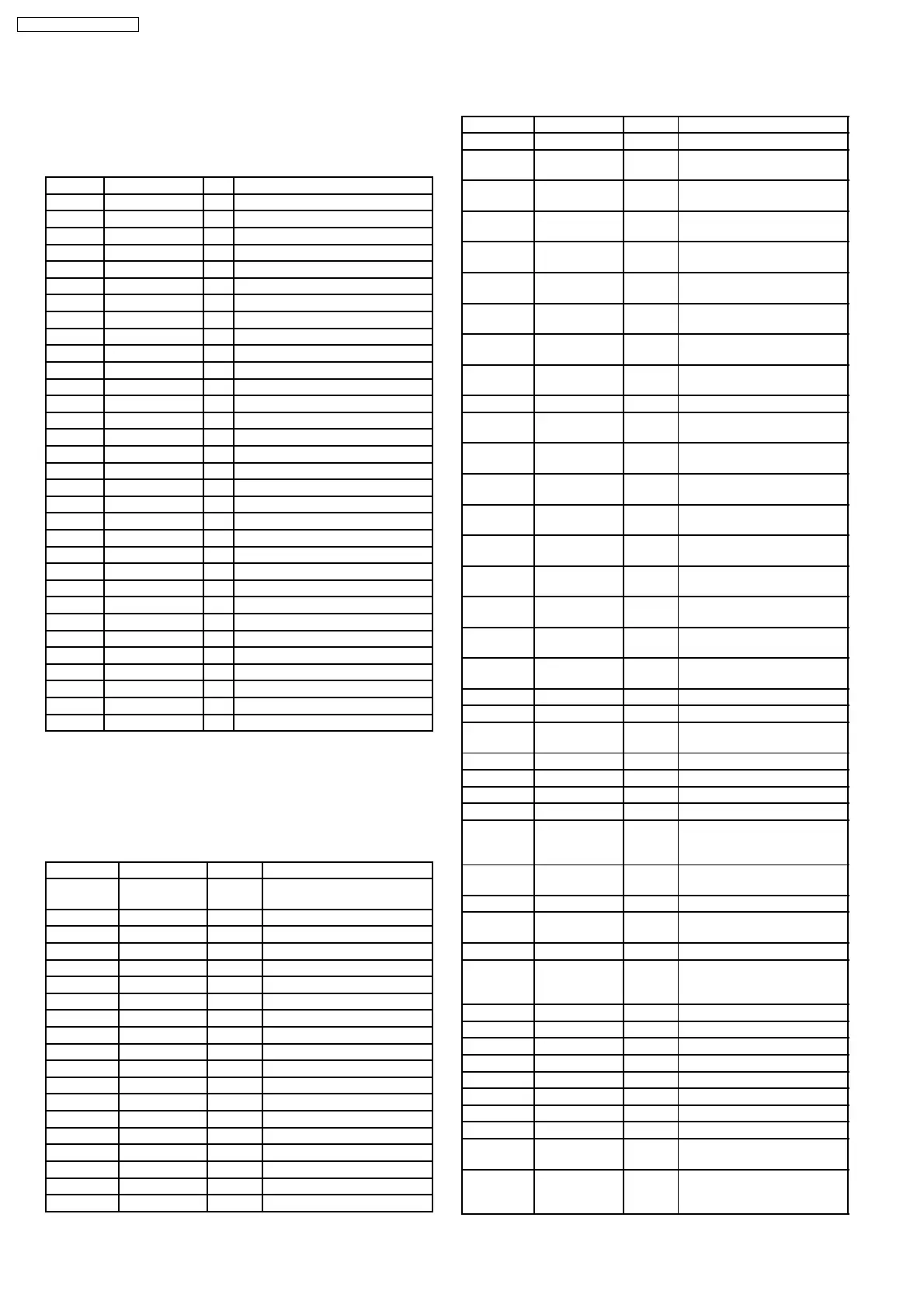
21.1. IC701 (AN22004A-NF) Servo
Amplifier
Pin No. Mark I/O Function
1 LPD I APC Amp input
2 LD I APC Amp output
3 VCC I Power supply
4 EQSW I Focus signal input terminal 1
5 RFOUT I RF summing output
6 RFIN I AGC input
7 CAGC O AGC Control
8 ARF O AGC output
9 CEA I Detector’s input
10 3TOUT I 3 T output
11 DCDET I Capacitor for HPF amp connection
12 OFTCONT O Capacitor 4 OFTR connection
13 BDO I BDO output (“H”: Drop_out)
14 OFTR O OFTR output
15 /RFDET O NRFDET output (“L” : detection)
16 LDON O Power-down input
17 GND - GND
18 EQ8ST O OFTR/BDO
19 VREF - VREF
20 TEN I TE Amp input
21 TEOUT I TE Amp output
22 FEN I FE Amp input
23 FEOUT O FE Amp output
24 GCTL O GCTL
25 FBAL I/O Focus Balance Control
26 TBAL O Tracking balance Control
27 E I Tracking balance control
28 F I Focus balance control
29 D I
30 B I
31 C I
32 A I
21.2. IC702 (MN6627934CH) Servo
Processor/ Digital Signal
Processor/ Digital Filter/ D/A
Converter
Pin No. Mark I/O Function
1 DRVDD - Power supply for DRAM
interface (Pin 2 to 19 and 80)
2 D0 I/O DRAM data I/O signal 0
3 D1 I/O DRAM data I/O signal 1
4 NEW O DRAM write enable signal
5 NRAS I/O DRAM RAS control signal
6 D2 I/O DRAM data I/O signal 2
7 D3 I/O DRAM data I/O signal 3
8 NCAS0 O DRAM CAS control signal 0
9 A10 O DRAM CAS control signal 10
10 A8 O DRAM address signal 8
11 A7 O DRAM address signal 7
12 A6 O DRAM address signal 6
13 A5 O DRAM address signal 5
14 A4 O DRAM address signal 4
15 A9 O DRAM address signal 9
16 A0 O DRAM address signal 0
17 A1 O DRAM address signal 1
18 A2 O DRAM address signal 2
19 A3 O DRAM address signal 3
Pin No. Mark I/O Function
20 DVSS2 - Ground for digital circuits
21 DVDD2 - Power supply for digital
cirfcuits
22 SPOUT O Spindle motor drive signal
output (absolute value output)
23 TRVP O Traverse drive output
(positive polarity output)
24 TRVM O Traverse drive output
(negative porarity output)
25 TRP O Tracking drive output (positive
polarity output)
26 TRM O Tracking drive output
(negative polarity output)
27 FOP O Focus drive output (positive
polarity output)
28 FOM O Focus drive output (negative
polarity output)
29 IOVDD1 - Power supply for I/O
30 TBAL O Tracking balance adjustment
output
31 FBAL O Focus balance adjustment
output
32 FE I Focus error signal input
(analog input)
33 TE I Tracking error signal input
(analog input)
34 RFENV I RF envelope signal input
(analog input)
35 OFT I Off-track signaL input High:
Off-track)
36 NRFDET I RF detection signal input
Low: detection
37 BDO I Dropout signal input
High: Dropout
38 LDON O Laser ON signal output
High: ON
39 ARF I RF signal input
40 IREF I Reference current input
41 ADPVCC I Voltage input for supply
voltage monitor (analog input)
42 DSLF O DSL loop filter
43 RFSW I DSL loop filter
44 PLLF O PLL loop filter
45 PLLFO O PLL loop filter
46 AVDD2 - Power supply for analog
circuits (for DSL, PLL and
A/D)
47 AVSS2 - Ground for analog circuits (for
DSL, PLL and A/D)
48 OUTL O L-ch audio output
49 AVSS1 - Ground for analog circuits (for
audio output stage)
50 OUTR O R-ch audio output
51 AVDD1 - Power supply for analog
circuits (for audio output
stage)
52 DVSS3 - Ground for digital circuits
53 DVDD3 - Power supply for digital circuit
54 TMOD2 I Test input pin Low: Normal
55 FLAG O Flag signal output
56 EXT2 I/O Expansion I/O port 2
57 EXT0 I/O Expansion I/O port 0
58 EXT1 I/O Expansion I/O port 1
59 IOVDD2 I Power supply for I/O
60 TX O Digital audio interface output
signal
61 MCLK I Micro controller command
clock signal input (Latches
data at the rising adge)
21 Terminal Function of IC’s
80
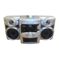
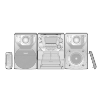
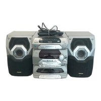
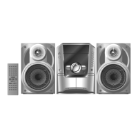
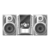
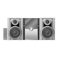
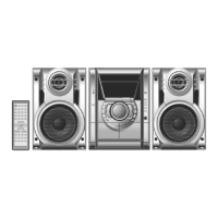
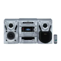
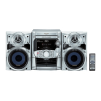
SA-AK220E / SA-AK220EB
 Loading...