EasyManua.ls Logo

Panasonic SA-G90 User Manual

Panasonic SA-G90
95 pages
To Next Page IconTo Next Page
Page #1 background imageLoading...
Page #1 background image
ORDER No.MD0004058C1
A2
Receiver
SA-G90
Colours
(K)...........Black Type
Areas
PP...........U.S.A. and Canada
SYSTEM : SC-S2350 for the U.S.A.
SC-S245 for Canada
SPECIFICATIONS
Specification
1
Question and Answer IconNeed help?

Do you have a question about the Panasonic SA-G90 and is the answer not in the manual?

Panasonic SA-G90 Specifications

General IconGeneral
TypeStereo receiver
Tuning rangeFM, MW
Power output45 watts per channel into 8Ω (stereo)
Frequency response20Hz to 20kHz
Total harmonic distortion0.07%
Dimensions430 x 125 x 300mm
Weight7.3kg
Channels2
BluetoothNo
HDMI InputsNo
USB PlaybackNo
FM TunerYes
Speaker load impedance8Ω to 16Ω

Summary

Specifications Overview

Specification Details

Detailed specifications for the audio receiver and its components.

Amplifier Section Specifications

FM Tuner Section Specifications

AM Tuner Section Specifications

Video Section Specifications

General Specifications

Safety Precautions

Insulation Resistance Test Procedure

Procedure for testing insulation resistance to prevent electric shock hazards.

Pre-Repair Procedures

Protection Circuitry Overview

Location of Controls Overview

Main Unit Controls

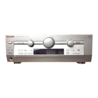
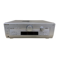
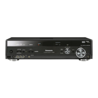
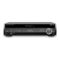
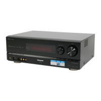
Identifies and describes controls and indicators on the main unit.

Remote Control Location

Remote Control Transmitter Functions

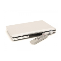
Describes the functions of buttons on the remote control transmitter.

Operation Checks and Component Replacement Procedures

PCB Checking Procedures

Guides for checking the FL, Surround, and IN/OUT terminal PCBs.

DTS P.C.B. Checking

Procedure for checking the DTS printed circuit board.

Main P.C.B. Checking

Procedure for checking the main printed circuit board.

Power IC and Regulator Transistor Replacement

Steps for replacing power ICs and regulator transistors.

Bottom Cover Installation

Instructions for installing the bottom cover after component replacement.

IC, Transistor, and Diode Type Illustrations

Schematic Diagram Overview

Schematic Diagram Notes

Key notes and explanations for understanding the schematic diagrams.

Schematic Diagram Symbols

Explanation of symbols used in schematic diagrams for signal lines.

Printed Circuit Board Diagrams

Block Diagram

Wiring Connection Diagram

IC Terminal Functions

IC901 System Microprocessor Terminals

Detailed terminal functions for the system microprocessor IC901.

Replacement Parts List

Cabinet Parts Location Diagram

Packaging Instructions

Power Transformer P.C.B. Layout

Power Supply P.C.B. Layout

Schematic Diagram-1

A IN/OUT TERMINAL CIRCUIT

Schematic for the audio and video input/output terminal circuit.

Schematic Diagram-2

G MAIN CIRCUIT

Schematic of the main audio processing and selector circuits.

Schematic Diagram-3

B SURROUND CIRCUIT

Schematic for the surround sound processing and digital input circuits.

Schematic Diagram-4

G MAIN CIRCUIT

Schematic of main audio control circuits including volume and sound controllers.

Schematic Diagram-5

B SURROUND CIRCUIT

Schematic for surround sound circuitry and related signal paths.

Schematic Diagram-6

C DTS CIRCUIT

Schematic diagram detailing the DTS processing circuitry.

Schematic Diagram-7

A IN/OUT TERMINAL CIRCUIT

Schematic for input/output terminals connecting to main circuit and tuner.

Schematic Diagram-8

D FL CIRCUIT

Schematic diagram for the FL display drive and related control circuits.

Schematic Diagram-9

FL P.C.B. Layout

Component layout for the FL display printed circuit board.

Schematic Diagram-10

D FL CIRCUIT

Schematic for FL display circuits including switches and tone controls.

Schematic Diagram-11

F HEADPHONES JACK CIRCUIT

Schematic diagram for the headphone jack and motor drive circuits.

Schematic Diagram-12

G MAIN CIRCUIT

Schematic of the main circuit, including EQ, selectors, and regulators.

Schematic Diagram-13

G MAIN CIRCUIT

Schematic for main circuit components like regulators and relays.

Schematic Diagram-14

G MAIN CIRCUIT

Schematic of main circuit power amplifiers and motor drive circuits.

Schematic Diagram-15

G MAIN CIRCUIT

Schematic for main circuit power amplifiers and associated components.

Schematic Diagram-16

G MAIN CIRCUIT

Schematic of the main circuit, including speaker outputs and protection.

H POWER SUPPLY CIRCUIT

Schematic for the power supply section of the unit.

I POWER TRANSFORMER CIRCUIT

Schematic for the power transformer and related circuitry.

J AC IN/OUT CIRCUIT

Schematic for AC input and output connections.

Schematic Diagram-17

Z120 TUNER UNIT (RAN0001MM)

Schematic diagram for the Z120 Tuner Unit.

Schematic Diagram-18

LA1844 FM/AM IF AMP, DET/AM OSC, MIX/FM MPX

Schematic for the LA1844 IC, handling FM/AM IF, detection, and mixing.

IC, Transistor, and Diode Type Illustrations

Power Supply P.C.B. Layout

Power Transformer P.C.B. Layout

AC IN/OUT P.C.B. Layout

Operation P.C.B. Layout

FL P.C.B. Layout

Headphones Jack P.C.B. Layout

IN/OUT Terminal P.C.B. Layout

Surround P.C.B. Layout

DTS P.C.B. Layout

IN/OUT Terminal P.C.B. Parts Location

Headphones Jack P.C.B. Parts Location

AC IN/OUT P.C.B. Parts Location

DTS P.C.B. Layout (Side A)

DTS P.C.B. Layout (Side B)

DTS P.C.B. Parts Location

Headphones Jack P.C.B. Parts Location

AC IN/OUT P.C.B. Parts Location

Surround P.C.B. Layout

Operation P.C.B. Parts Location

Surround P.C.B. Parts Location

FL P.C.B. Parts Location

FL P.C.B. Parts Location

Main P.C.B. Layout

Main P.C.B. Parts Location

Related product manuals