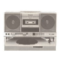
14. Wiring Connection Diagram
15. Block Diagram
16. Terminal Function of ICs
16.1. IC502(C2CBKJ000061): / System Control
Pin
No.
Terminal
Name
I/O Function
1
EEPROM
/ SDA
I Date signal output for IC501
2
EEPROM
/ SCL
O Clock signal output for IC501
3
EEPROM
/ WP
O WP signal output for IC501
4 NC - Not used, open
5 DC IN I Power failure detect signal input
6 NC - Not used, open
7 NC - Not used, open
8 NC -
Connected to V
SS
9
CNV
SS
-
Connected to V
SS
via resistor
10 NC - Not used, open
11 NC - Not used, open
12 NRST I Reset signal input
13 XOUT O Oscillator connected terminal (F
=10 MHz)
14
V
SS
- GND
15 XIN I Oscillator connected terminal (F
=10 MHz)
16
V
CC
I Power supply terminal
17 NC -
Not used, connected to V
CC
via
resistor
18
DSP /
STATUS
I Status signal input from IC401
19
DSP /
LOCK
I Lock detect signal input for
IC401
20
REMO /
CON
I Remote control signal input
21
FAN /
ON/OFF
O Fan motor drive signal input
22
FAN /
SPEED
O Fan motor rotation speed
control
23
/ERR /
RCVY
O Error recovery signal output
18