Switching
Door sta 2
detection
circuit
Door sta 1
detection
circuit
Door
Opener
1
Door
Opener
2
2
22
2
2
2
2
2
2
2
2
CN600
Power supply
circuit for door sta
+22V
+12V
V5A
FM power
supply circuit
NTSC Signal
VDD33 3VB
(X390)
32kHz
VDD33
+
VDD33
VDD33
VDD33
SPI 1
SPI 3
UART2
UART1
UART 3
SPI 2
DPJP3
IC100
Main CPU
VDD12
VDD33
VDD12
1.2V DCDC
SDRAM
(128Mbit)
(IC300)
SCLK,SDA
CKE,CLK,UB,LB,CS,RAS,
CAS,WE
ABUS[0-15]
DBUS[0-15]
RTC
I
2
C
FM demodulation/
ASK communication
(IC670)
Switching
AMP
AM Signal
AM communication
circuit
Debug
Serial
BBIC
Serial
BBRX( )
AM
communication
circuit
External input
External input
External input 1
External input 2
DC/DC
circuit
DC/D
VDD40 +4VRF
+4VSP
BB1.8V
VDD33
RF3.2V
BB3.3V
BB1.8V
AVDD33
VDD50
22V
SP
(IC801)
(IC582)
(IC760)
(IC582)
(IC500)
AMP
AMP
AMP
AMP
AMP
AMP
MIC
+12V
3.3VREG
DC/D
DC/D
Electric Lock
control 1
Electric Lock
control 2
Electric Lock
Electric Lock
Sub monitor IN
Sub monitor OUT
Sub monitor OUT
Sub monitor OUT
Power supply
for Core
Power supply
for I/O
Power supply
for RF
VDDIO_EBI
BB3.3V
BB1.8V
BB1.8V
JTAG
BBIC_TX_RES,BBIC_TX
BBIC_RX_RES,BBIC_RX,BBIC_nFREEZE
LCD_HD,LCD_VD,LCD_CLK,LCDC_TX.
LCDC_CK.LCDC_CS,LCD_nRST
VDD33
(CN200)
7''
800 480
WVGA
LCD
QSPI(128Mbit)
LCD_R[0-7],LCD_G[0-7]
BBIC_SPI_TX,BBIC_SPI_CLK,
BBIC_SPI_RX
Debug Serial
DBGD,DGBC
RSTB
LED[1]
Debug
Serial
AM32
JTAG
VDD33
VDD60
RESET_SW
(SW100)
27MHz
(X380)
STOP
BL_ON
BL circuit
(IC270)
To uc h
Controller
(IC1002)
DC/DC
(IC1001)
PAD PAD
V12
TALK
KEY_RST
I2C_SDA
I2C_SCL
KEY INT
RST
GND
+5V
SDA
SCL
INT
RST
IC
(IC101)
BB_nRST
J2_CONT
A2_IN
A1_IN
BBIC_DOWNLD
AM2_TX,AM2_RX
AM_RX
MODE_SE
(IC160)
(IC642)
J1_CONT
BBTX( ), BBRX( )
(IC500)
JTAG
QSPI(8Mbit)
D[0-15]
A[1-16]
SRAMCS
10.368MH
(X401)
EEPROM(64Kbit)
(IC401)
SRAM(1Mbitor2Mbit)
(IC404)
CA_CALL
V_SEL1*
2
V_SEL2*
CB_CALL
SUB_TALKON
LOGIC_CNT
EXV_CNT1
EXV_CNT2
LOGIC_CNT
DPH_SEL1
CAM_PWR
MODE_SEL
AM_TX
AM_PWM
LINE_Z
DOUT_IN
FM_ON
AM_TX
AM_RX
AM_PWM
PBX_IF
Power Board
Key Board
CN601
PS241
PBX I/F
Sub CPU
IC405
20
6
URAT_CNT
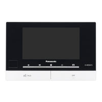
VL-MV75 : Main monitor station diagram
24V
 Loading...