Circuit Descriptions
EN 24 TPM8.3L LA7.
2011-Sep-30
7.4 Circuit Description
7.4.1 System power
The main board power is received at connector CN701 from
power board, to receive the power and signals from the PSU.
See Table 7-1
for the correct pining, The shown test points in
Figure 7-4
.
Table 7-1 Connector CN701 overview
Figure 7-4 System power
7.4.2 Nand flash Memory (U403)
The set uses a 256 MB NAND flash for software code
Figure 7-5 Nand flash Memory (U403)
7.4.3 NVM (U4103)
The system NVM is a 128 KB IC. It contains all system settings.
Figure 7-6 NVM (U4103)
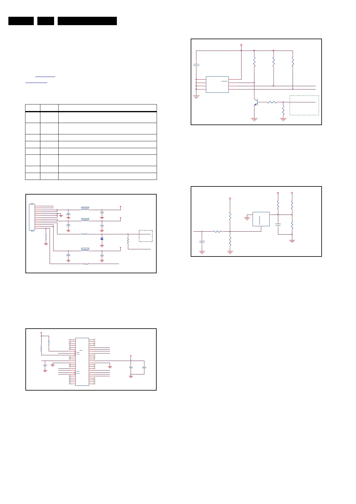
7.4.4 Reset (U4101)
When the input voltage for the MT5301B main processor drops
below 2.93 V, a system reset will be enforced by U4101.
Figure 7-7 Reset (U4101)
Item Pin Description
1 1 INVERTER_ON_OFF, Inverter board
control (Low: ON, High: OFF)
2 2 BRIGHT_ADJ, Inverter bright PWM
control (Max.: 0 V, Min.: 3V3)
3 3, 4 +12 V Supply
4 5, 6, 7 Ground
5 8, 9 +24 V Supply
6 10 STANDBY, Standby
control (High: Normal, Low: Stand by)
7 11, 12 STB_PWR5V, +5VSB Supply
8 13 POWER OK
19190_208_110905.eps
110905
C706
10uF 10V
NC/C702
100N 50V
BL_CTRL
BRI_ADJ
+
C703
330UF 35V
R738
NC/0R05 1/16W
PWR_OK
+
C705
470UF 10V
CN701
CONN
1
2
3
4
5
6
7
8
9
10
11
12
13
R701
10K 1/16W 5%
FB702
120R/6000mA
1 2
C704
100N 50V
ZD701
NC/BZX84C3V6
1 3
+24V
H : ON
L : Standby
+
NC/C701
330UF 35V
+12V
FB703
120R/6000mA
1 2
PSU_STBY
R750
0R05 1/10W
R712
8.2K 1/10W
OPWRSB
NC/FB701
120R/6000mA
1 2
5VSB
19190_211_110905.eps
110905
PDD2
DV DD3V3
PDD6
PDD3
PDD5
PACLE
POOE#
U403
HY27US08561A-TPCB
39
1
2
3
4
5
46
17
16
18
26
11
19
7
14
15
27
28
20
21
22
32
33
36
12
8
37
31
30
29
13
45
44
43
42
41
40
23
24 25
9
34
35
47
38
6
10
48
NC23
NC1
NC2
NC3
NC4
NC5
NC26
ALE
CLE
WE
NC17
NC8
WP
RY/BY1
NC9
NC10
NC18
NC19
NC11
NC12
NC13
I/O3
NC20
VSS2
VCC1
RE
VCC2
I/O2
I/O1
I/O0
VSS1
NC25
I/O7
I/O6
I/O5
I/O4
NC24
NC14
NC15 NC16
CE1
NC21
NC22
NC27
PRE
NC6
NC7
NC28
PDD0
PDD1
PAALE
C4109
100N 16V
DVDD3V3
DV DD3V3
PDD4
PDD7
R4117
4K7 1/16W 5%
C4108
100N 16V
PARB#
DVDD3V3
POWE#
C4110
10uF 10V
FLASH_WP#
POCE1#
R4115
4K7 1/16W 5%
19190_212_110905.eps
110905
U4103
CAT24C128YI
4
8
5
6
1
2
3
7
VSS
VCC
SDA
SCL
E0
E1
E2
WC
R4105
2.7K 1/16W 1%
R4103
10K 1/16W 5%
DVDD3V3
I2C address at A0
R4104
2.7K 1/16W 1%
H: Write Enable
R4106
2.2K 1/16W
C4104
220N16V
OSCL0
R4109
10K 1/16W 5%
Q4101
PMBS3904
L: Write Protect
MEMORY _WP#
OSDA0
19190_213_110905.eps
110905
R4110
NC/100K 1/16W
C4123
NC/10P 50V
R4108
0R05 1/16W
R4111
NC/820R 1/10W 1%
R4139
0R05 1/16W
C4107
100N 16V
R4112
NC/1K8 1/10W 1%
R4140
NC/5K1 1/16W 5%
ORESET#
3V3SB
U4101
MAX809STRG
1
2
3
GND
RESET
VCC
3V3SB
5VSB
 Loading...