Faultfinding Guide
GB 61CDR779 8.
8.2.6 Oscillograms
Figure 8-14
8.2.7 Circuit description
Input circuit
The input circuit consists of a lightning protection circuit and
an EMI filter.
The lightning protection comprises R3120, gasarrestor 1125
and R3124.
The EMI filter is formed by C2120, L5120, C2125 and R3124.
It prevents inflow of noise into/from the mains.
Primary rectifier/smoothing circuit
The AC input is rectified by rectifier bridge 6102 and
smoothed into C2121. The voltage over C2121 is
approximately 300V. It can vary from 100V to 390V.
Start circuit and Vcc supply
This circuit is formed by R3123, R3134, C2129, D6129,
R3129, R3111, C2133 and C2111.
When the power plug is connected to the mains voltage, the
stabilised voltage over D6129(24V) will charge C2133 via
R3129. When the voltage reaches 14,5V across C2111, the
control circuit of IC7110 is turned on and the regulation
starts. During regulation, Vcc of IC7110 will be supplied by
the rectified voltage from winding 7-9 via L5132, D6132 and
C2133.
Control circuit
The control circuit exists of IC7110, C2102, C2104, C2107,
C2109, C2110, R3102, R3103, R3104, R3107, R3108,
R3109 and R3110. C2102 and R3110 define the frequency
of the oscillator.
Power switch circuit
This circuit comprises MOSFET 7125, Rsense 3126, 3127
and 3128, R3125, C2127, L5125, R3112 and R3113. R3125
is a pull-down resistor to remove static charges from the gate
of the MOSFET.
Regulation circuit
The regulation circuit comprises opto-coupler 7200 which
isolates the error signal from the control IC on the primary
side and a reference component 7201. The TL431(7201) can
be represented by two components:
• a very stable and accurate reference diode
• a high gain amplifier
Figure 8-15
TL431 will conduct from cathode to anode when the
reference is higher than the internal reference voltage of
about 2.5V. If the reference voltage is lower, the cathode
current is almost zero.
The cathode current flows through the LED of the opto-
coupler. The collector current of the opto-coupler flows
through R3106, producing an error voltage, connected to
voltage feedback pin 14 of IC7110.
Overvoltage protection circuit
This circuit consist of D6114, C2114, R3115and R3116.
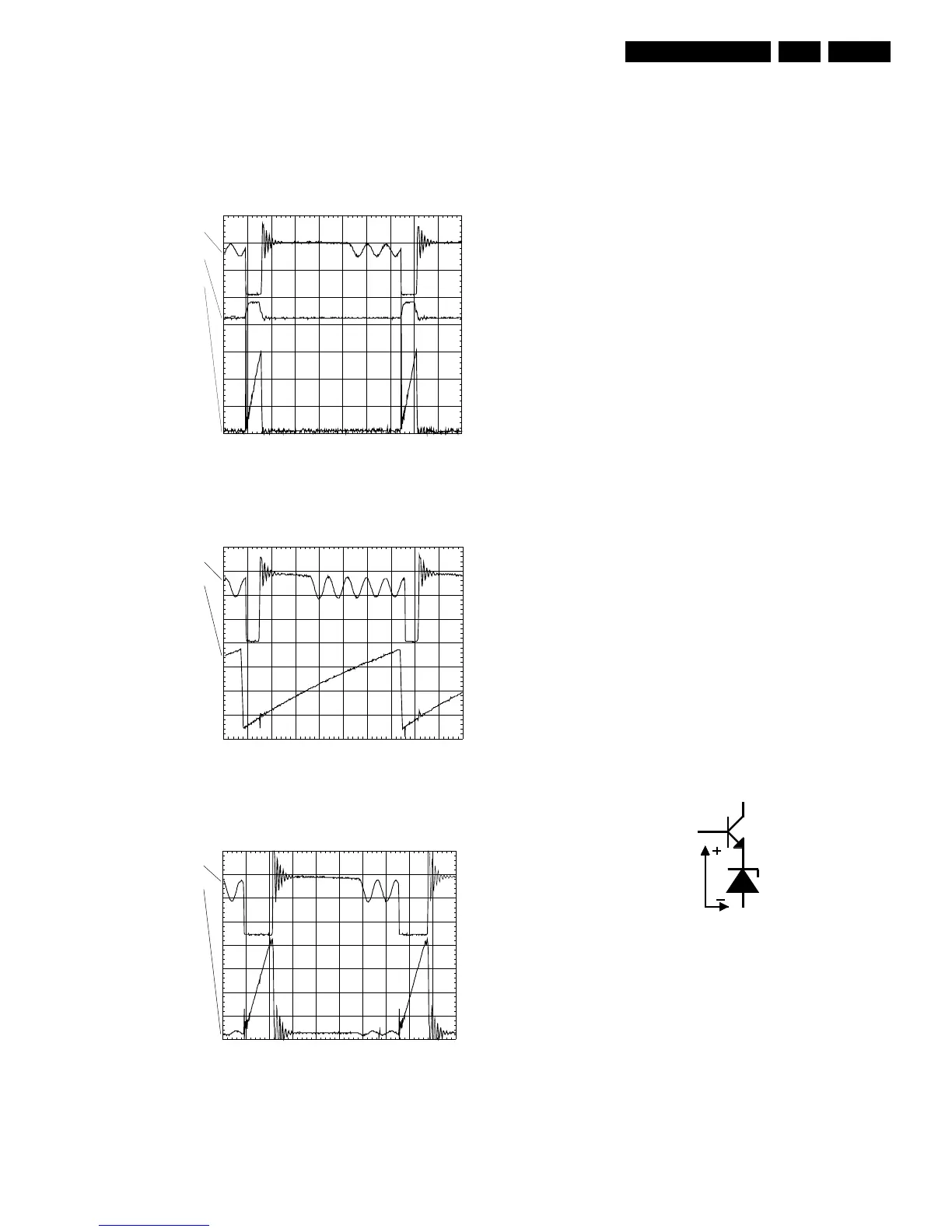
Oscillograms
PM3394B
ch2
ch3
ch1
CH1 2
CH2
CH3 2 V~ ALT MTB5.00us- 0.90dv ch1-
1
2
3
T
ch1 : Drain voltage
ch2 : Drain current
ch3 : Gate voltage
PM3394B
ch3
ch1
CH1 1
CH3 50mV~ ALT MTB5.00us- 0.90dv ch1-
1
3
T
ch1 : Drain voltage
ch2 : Oscillator voltage
PM3394B
ch3
ch1
CH1 1
CH3 20mV~ ALT MTB5.00us- 0.90dv ch1-
1
3
T
ch1 : Drain voltage
ch3 : Sense voltage
CL 06532151_022.eps
301100
A
2.5V
R
K
CL 06532151_023.eps
271100